The Intel i960 was a remarkable 32-bit processor of the 1990s with a confusing set of versions. Although it is now mostly forgotten (outside the many people who used it as an embedded processor), it has a complex history. It had a shot at being Intel's flagship processor until x86 overshadowed it. Later, it was the world's best-selling RISC processor. One variant was a 33-bit processor with a decidedly non-RISC object-oriented instruction set; it became a military standard and was used in the F-22 fighter plane. Another version powered Intel's short-lived Unix servers. In this blog post, I'll take a look at the history of the i960, explain its different variants, and examine silicon dies. This chip has a lot of mythology and confusion (especially on Wikipedia), so I'll try to clear things up.
Roots: the iAPX 432
The ancestry of the i960 starts in 1975, when Intel set out to design a "micro-mainframe", a revolutionary processor that would bring the power of mainframe computers to microprocessors. This project, eventually called the iAPX 432, was a huge leap in features and complexity. Intel had just released the popular 8080 processor in 1974, an 8-bit processor that kicked off the hobbyist computer era with computers such as the Altair and IMSAI. However, 8-bit microprocessors were toys compared to 16-bit minicomputers like the PDP-11, let alone mainframes like the 32-bit IBM System/370. Most companies were gradually taking minicomputer and mainframe features and putting them into microprocessors, but Intel wanted to leapfrog to a mainframe-class 32-bit processor. The processor would make programmers much more productive by bridging the "semantic gap" between high-level languages and simple processors, implementing many features directly into the processor.
The 432 processor included memory management, process management, and interprocess communication. These features were traditionally part of the operating system, but Intel built them in the processor, calling this the "Silicon Operating System". The processor was also one of the first to implement the new IEEE 754 floating-point standard, still in use by most processors. The 432 also had support for fault tolerance and multi-processor systems. One of the most unusual features of the 432 was that instructions weren't byte aligned. Instead, instructions were between 6 and 321 bits long, and you could jump into the middle of a byte. Another unusual feature was that the 432 was a stack-based machine, pushing and popping values on an in-memory stack, rather than using general-purpose registers.
The 432 provided hardware support for object-oriented programming, built around an unforgeable object pointer called an Access Descriptor. Almost every structure in a 432 program and in the system itself is a separate object. The processor provided fine-grain security and access control by checking every object access to ensure that the user had permission and was not exceeding the bounds of the object. This made buffer overruns and related classes of bugs impossible, unlike modern processors.
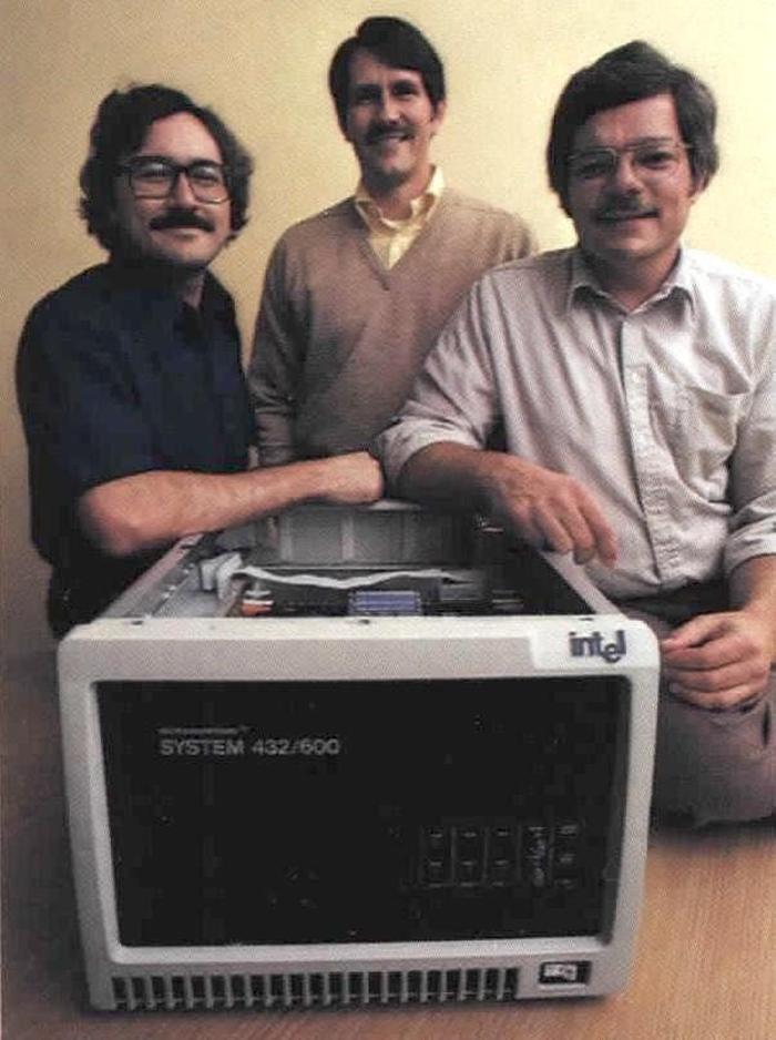
This photo from the Intel 1981 annual report shows Intel's 432-based development computer and three of the engineers.
The new, object-oriented Ada language was the primary programming language for the 432. The US Department of Defense developed the Ada language in the late 1970s and early 1980s to provide a common language for embedded systems, using the latest ideas from object-oriented programming. Proponents expected Ada to become the dominant computer language for the 1980s and beyond. In 1979, Intel realized that Ada was a good target for the iAPX 432, since they had similar object and task models. Intel decided to "establish itself as an early center of Ada technology by using the language as the primary development and application language for the new iAPX 432 architecture." The iAPX 432's operating system (iMAX 432) and other software were written in Ada, using one of the first Ada compilers.
Unfortunately, iAPX 432 project was way too ambitious for its time. After a couple of years of slow progress, Intel realized that they needed a stopgap processor to counter competitors such as Zilog and Motorola. Intel quickly designed a 16-bit processor that they could sell until the 432 was ready. This processor was the Intel 8086 (1978), which lives on in the x86 architecture used by most computers today. Critically, the importance of the 8086 was not recognized at the time. In 1981, IBM selected Intel's 8088 processor (a version of the 8086 with an 8-bit bus) for the IBM PC. In time, the success of the IBM PC and compatible systems led to Intel's dominance of the microprocessor market, but in 1981 Intel viewed the IBM PC as just another design win. As Intel VP Bill Davidow later said, "We knew it was an important win. We didn't realize it was the only win."
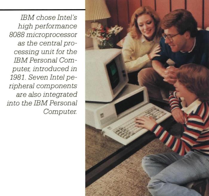
Caption: IBM chose Intel's high performance 8088 microprocessor as the central processing unit for the IBM Personal Computer, introduced in 1981. Seven Intel peripheral components are also integrated into the IBM Personal Computer. From Intel's 1981 annual report.
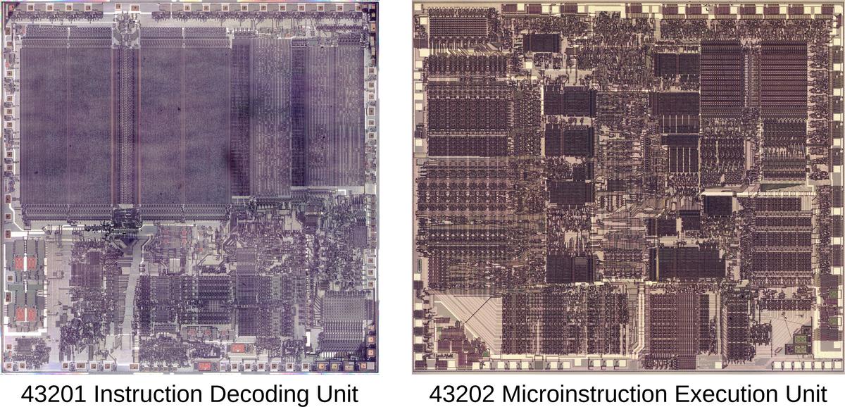
Intel finally released the iAPX 432 in 1981. Intel's 1981 annual report shows the importance of the 432 to Intel. A section titled "The Micromainframe™ Arrives" enthusiastically described the iAPX 432 and how it would "open the door to applications not previously feasible". To Intel's surprise, the iAPX 432 ended up as "one of the great disaster stories of modern computing" as the New York Times put it. The processor was so complicated that it was split across two very large chips:1 one to decode instructions and a second to execute them Delivered years behind schedule, the micro-mainframe's performance was dismal, much worse than competitors and even the stopgap 8086.2 Sales were minimal and the 432 quietly dropped out of sight.
My die photos of the two chips that make up the iAPX 432 General Data Processor. Click for a larger version.
Intel picks a 32-bit architecture (or two, or three)
In 1982, Intel still didn't realize the importance of the x86 architecture. The follow-on 186 and 286 processors were released but without much success at first.3 Intel was working on the 386, a 32-bit successor to the 286, but their main customer IBM was very unenthusiastic.4 Support for the 386 was so weak that the 386 team worried that the project might be dead.5 Meanwhile, the 432 team continued their work. Intel also had a third processor design in the works, a 32-bit VAX-like processor codenamed P4.6
Intel recognized that developing three unrelated 32-bit processors was impractical and formed a task force to develop a Single High-End Architecture (SHEA). The task force didn't achieve a single architecture, but they decided to merge the 432 and the P4 into a processor codenamed the P7, which would become the i960. They also decided to continue the 386 project. (Ironically, in 1986, Intel started yet another 32-bit processor, the unrelated i860, bringing the number of 32-bit architectures back to three.)
At the time, the 386 team felt that they were treated as the "stepchild" while the P7 project was the focus of Intel's attention. This would change as the sales of x86-based personal computers climbed and money poured into Intel. The 386 team would soon transform from stepchild to king.5
The first release of the i960 processor
Meanwhile, the 1980 paper The case for the Reduced Instruction Set Computer proposed a revolutionary new approach for computer architecture: building Reduced Instruction Set Computers (RISC) instead of Complex Instruction Set Computers (CISC). The paper argued that the trend toward increasing complexity was doing more harm than good. Instead, since "every transistor is precious" on a VLSI chip, the instruction set should be simplified, only adding features that quantitatively improved performance.
The RISC approach became very popular in the 1980s. Processors that followed the RISC philosophy generally converged on an approach with 32-bit easy-to-decode instructions, a load-store architecture (separating computation instructions from instructions that accessed memory), straightforward instructions that executed in one clock cycle, and implementing instructions directly rather than through microcode.
The P7 project combined the RISC philosophy and the ideas from the 432 to create Intel's first RISC chip, originally called the 809607 and later the i960. The chip, announced in 1988, was significant enough for coverage in the New York Times. Analysts said that the chip was marketed as an embedded controller to avoid stealing sales from the 80386. However, Intel's claimed motivation was the size of the embedded market; Intel chip designer Steve McGeady said at the time, "I'd rather put an 80960 in every antiskid braking system than in every Sun workstation.” Nonetheless, Intel also used the i960 as a workstation processor, as will be described in the next section.
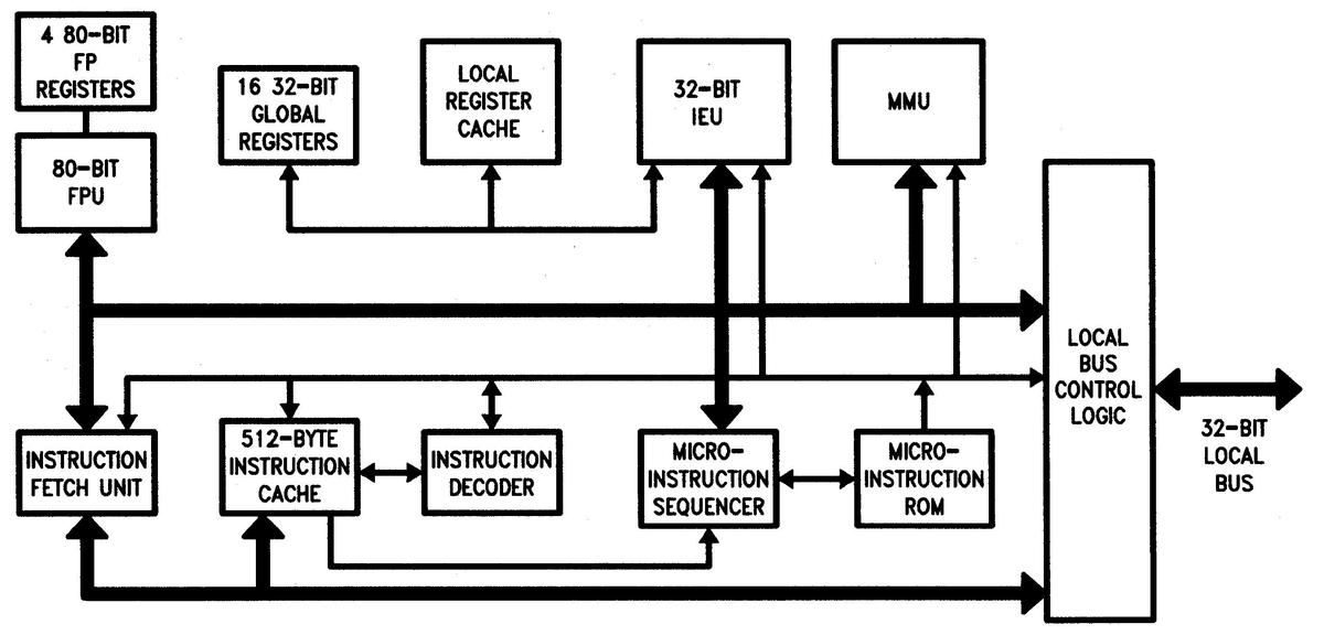
The block diagram below shows the microarchitecture of the original i960 processors. The microarchitecture of the i960 followed most (but not all) of the common RISC design: a large register set, mostly one-cycle instructions, a load/store architecture, simple instruction formats, and a pipelined architecture. The Local Register Cache contains four sets of the 16 local registers. These "register windows" allow the registers to be switched during function calls without the delay of saving registers to the stack. The micro-instruction ROM and sequencer hold microcode for complex instructions; microcode is highly unusual for a RISC processor. The chip's Floating Point Unit8 and Memory Management Unit are advanced features for the time.
The microarchitecture of the i960 XA. FPU is Floating Point Unit. IEU is Instruction Execution Unit. MMU is Memory Management Unit. From the 80960 datasheet.
It's interesting to compare the i960 to the 432: the programmer-visible architectures are completely different, while the instruction sets are almost identical.9 Architecturally, the 432 is a stack-based machine with no registers, while the i960 is a load-store machine with many registers. Moreover, the 432 had complex variable-length instructions, while the i960 uses simple fixed-length load-store instructions. At the low level, the instructions are different due to the extreme architectural differences between the processors, but otherwise, the instructions are remarkably similar, modulo some name changes.
The key to understanding the i960 family is that there are four architectures, ranging from a straightforward RISC processor to a 33-bit processor implementing the 432's complex instruction set and object model.10 Each architecture adds additional functionality to the previous one:
- The Core architecture consists of a "RISC-like" core.
- The Numerics architecture extends Core with floating-point.
- The Protected architecture extends Numerics with paged memory management, Supervisor/User protection, string instructions, process scheduling, interprocess communication for OS, and symmetric multiprocessing.
- The Extended architecture extends Protected with object addressing/protection and interprocess communication for applications. This architecture used an extra tag bit, so registers, the bus, and memory were 33 bits wide instead of 32.
These four versions were sold as the KA (Core), KB (Numerics), MC (Protected), and XA (Extended). The KA chip cost $174 and the KB version cost $333 while MC was aimed at the military market and cost a whopping $2400. The most advanced chip (XA) was, at first, kept proprietary for use by BiiN (discussed below), but was later sold to the military. The military versions weren't secret, but it is very hard to find documentation on them.11
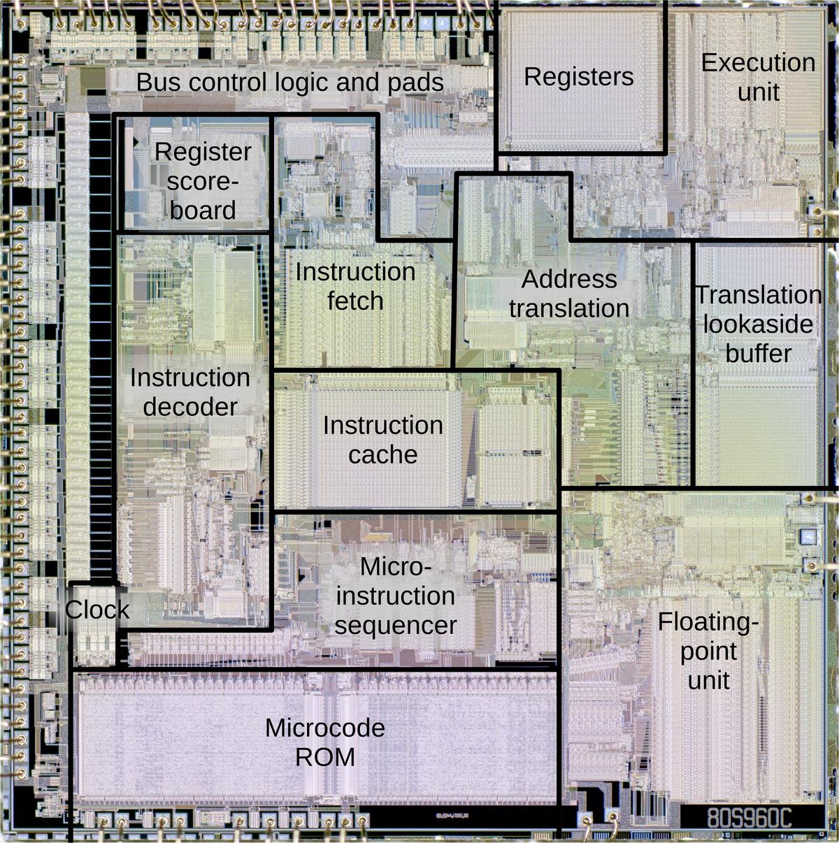
The strangest thing about these four architectures is that the chips were identical, using the same die. In other words, the simple Core chip included all the circuitry for floating point, memory management, and objects; these features just weren't used.12 The die photo below shows the die, with the main functional units labeled. Around the edge of the die are the bond pads that connect the die to the external pins. Note that the right half of the chip has almost no bond pads. As a result, the packaged IC had many unused pins.13
The i960 KA/KB/MC/XA with the main functional blocks labeled. Click this image (or any other) for a larger version. Die image courtesy of Antoine Bercovici. Floorplan from The 80960 microprocessor architecture.
One advanced feature of the i960 is register scoreboarding, visible in the upper-left corner of the die. The idea is that loading a register from memory is slow, so to improve performance, the processor executes the following instructions while the load completes, rather than waiting. Of course, an instruction can't be executed if it uses a register that is being loaded, since the value isn't there. The solution is a "scoreboard" that tracks which registers are valid and which are still being loaded, and blocks an instruction if the register isn't ready. The i960 could handle up to three outstanding reads, providing a significant performance gain.
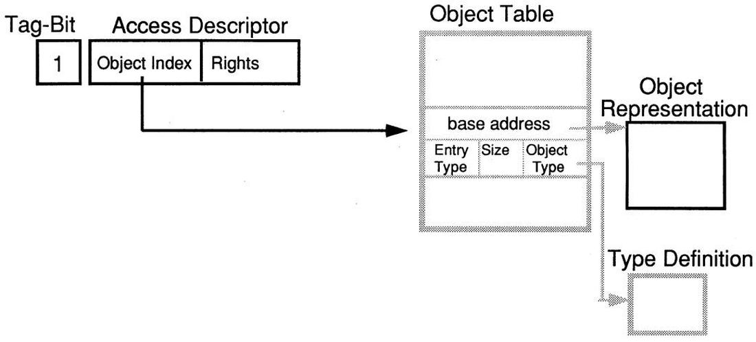
The most complex i960 architecture is the Extended architecture, which provides the object-oriented system. This architecture is designed around an unforgeable pointer called an Access Descriptor that provides protected access to an object. What makes the pointer unforgeable is that it is 33 bits long with an extra bit that indicates an Access Descriptor. You can't set this bit with a regular 32-bit instruction. Instead, an Access Descriptor can only be created with a special privileged instruction, "Create AD".14
The diagram above shows how objects work. The 33-bit Access Descriptor (AD) has its tag bit set to 1, indicating that it is a valid Access Descriptor. The Rights field controls what actions can be performed by this object reference. The AD's Object Index references the Object Table that holds information about each object. In particular, the Base Address and Size define the object's location in memory and ensure that an access cannot exceed the bounds of the object. The Type Definition defines the various operations that can be performed on the object. Since this is all implemented by the processor at the instruction level, it provides strict security.
Gemini and BiiN
The i960 was heavily influenced by a partnership called Gemini and then BiiN. In 1983, near the start of the i960 project, Intel formed a partnership with Siemens to build high-performance fault-tolerant servers. In this partnership, Intel would provide the hardware while Siemens developed the software. This partnership allowed Intel to move beyond the chip market to the potentially-lucrative systems market, while adding powerful systems to Siemens' product line. The Gemini team contained many of the people from the 432 project and wanted to continue the 432's architecture. Gemini worked closely with the developers of the i960 to ensure the new processor would meet their needs; both teams worked in the same building at Intel's Jones Farm site in Oregon.
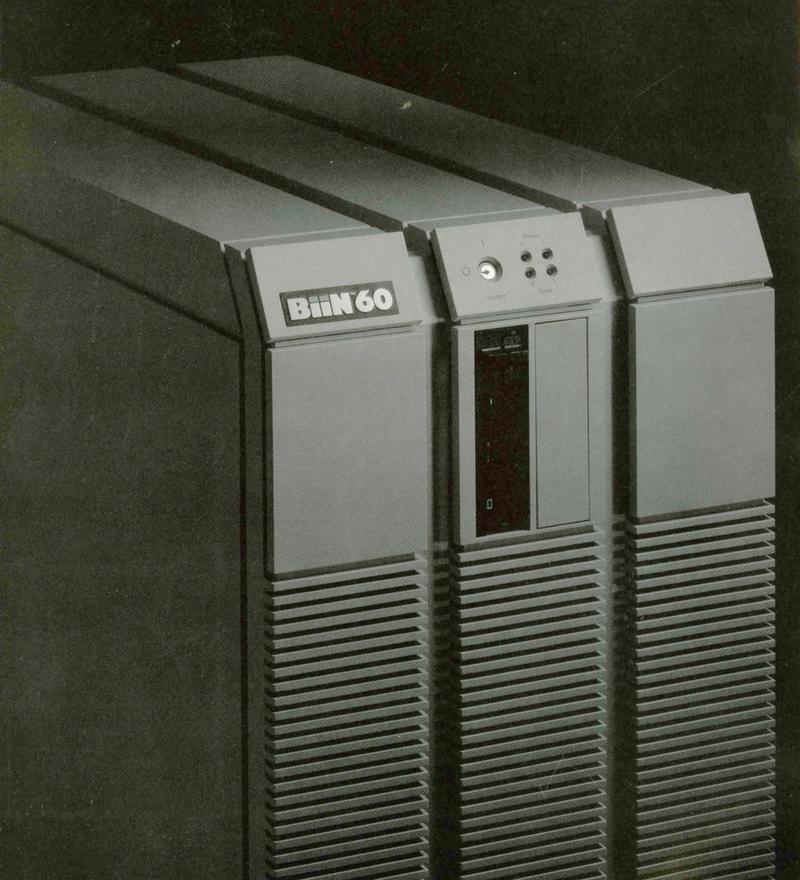
In 1988, shortly after the announcement of the i960 chips, the Intel/Siemens partnership was spun off into a company called BiiN.15 BiiN announced two high-performance, fault-tolerant, multiprocessor systems. These systems used the i960 XA processor16 and took full advantage of the object-oriented model and other features provided by its Extended architecture. The BiiN 20 was designed for departmental computing and cost $43,000 to $80,000. It supported 50 users (connected by terminals) on one 5.5-MIPS i960 processor. The larger BiiN 60 handled up to 1000 terminals and cost $345,000 to $815,000. The Unix-compatible BiiN operating system (BiiN/OS) and utilities were written in 2 million lines of Ada code.
BiiN described many potential markets for these systems: government, factory automation, financial services, on-line transaction processing, manufacturing, and health care. Unfortunately, as ExtremeTech put it, "the market for fault-tolerant Unix workstations was approximately nil." BiiN was shut down in 1989, just 15 months after its creation as profitability kept becoming more distant. BiiN earned the nickname "Billions invested in Nothing"; the actual investment was 1700 person-years and $430 million.
The superscalar i960 CA
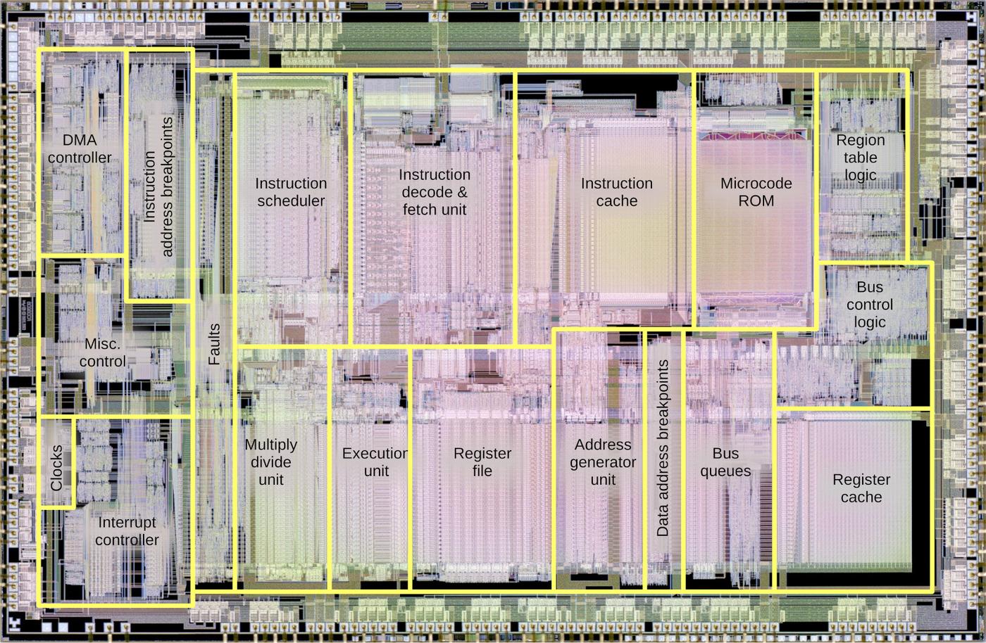
One year after the first i960, Intel released the groundbreaking i960 CA. This chip was the world's first superscalar microprocessor, able to execute more than one instruction per clock cycle. The chip had three execution units that could operate in parallel: an integer execution unit, a multiply/divide unit, and an address generation unit that could also do integer arithmetic.17 To keep the execution units busy, the i960 CA's instruction sequencer examined four instructions at once and determined which ones could be issued in parallel without conflict. It could issue two instructions and a branch each clock cycle, using branch prediction to speculatively execute branches out of order.
The i960 CA die, with functional blocks labeled. Photo courtesy of Antoine Bercovici. Functional blocks from the datasheet.
Following the CA, several other superscalar variants were produced: the CF had more cache, the military MM implemented the Protected architecture (memory management and a floating point unit), and the military MX implemented the Extended architecture (object-oriented).
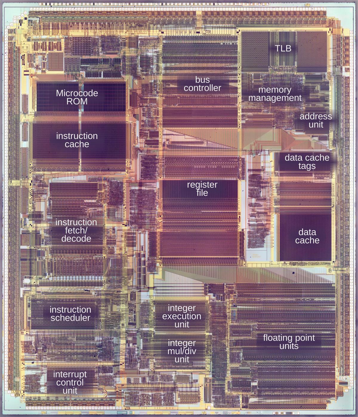
The image below shows the 960 MX die with the main functional blocks labeled. (I think the MM and MX used the same die but I'm not sure.18) Like the i960 CA, this chip has multiple functional units that can be operated in parallel for its superscalar execution. Note the wide buses between various blocks, allowing high internal bandwidth. The die was too large for the optical projection of the mask, with the result that the corners of the circuitry needed to be rounded off.
The i960MX die with the main functional blocks labeled. This is a die photo I took, with labels based on my reverse engineering.
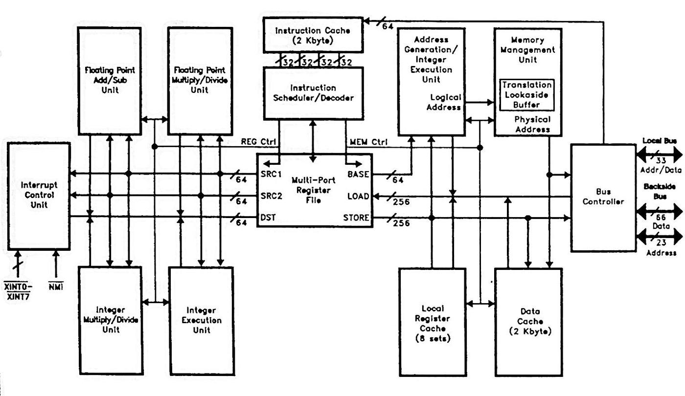
The block diagram of the i960 MX shows the complexity of the chip and how it is designed for parallelism. The register file is the heart of the chip. It is multi-ported so up to 6 registers can be accessed at the same time. Note the multiple, 256-bit wide buses between the register file and the various functional units. The chip has two buses: a high-bandwidth Backside Bus between the chip and its external cache and private memory; and a New Local Bus, which runs at half the speed and connects the chip to main memory and I/O. For highest performance, the chip's software would access its private memory over the high-speed bus, while using the slower bus for I/O and shared memory accesses.
A functional block diagram of the i960 MX. From Intel Military and Special Projects Handbook, 1993.
Military use and the JIAWG standard
The i960 had a special role in the US military. In 1987 the military mandated the use of Ada as the single, common computer programming language for Defense computer resources in most cases.19 In 1989, the military created the JIAWG standard, which selected two 32-bit instruction set architectures for military avionics. These architectures were the i960's Extended architecture (implemented by the i960 XA) and the MIPS architecture (based on a RISC project at Stanford).20 The superscalar i960 MX processor described earlier soon became a popular JIAWG-compliant processor, since it had higher performance than the XA.
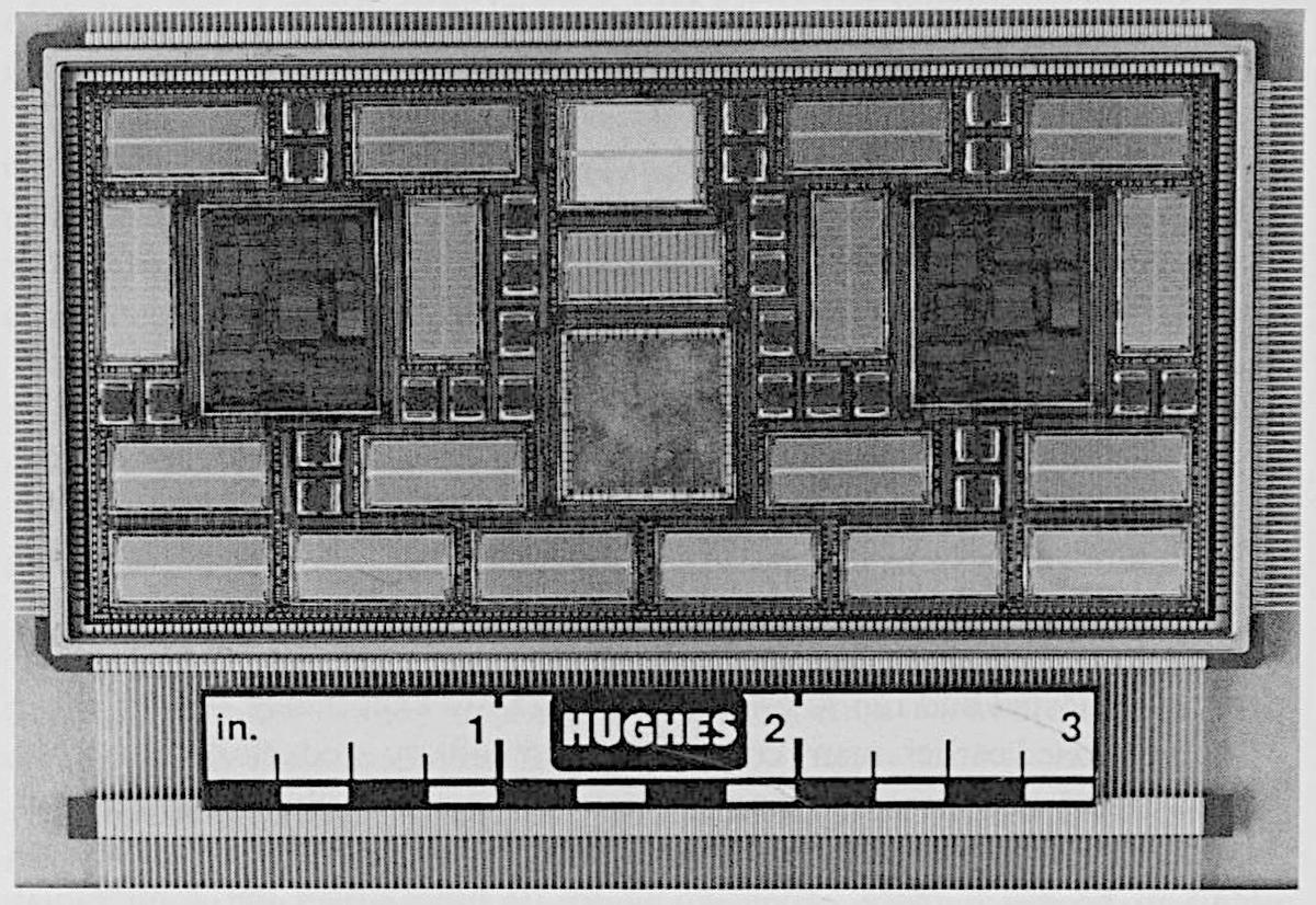
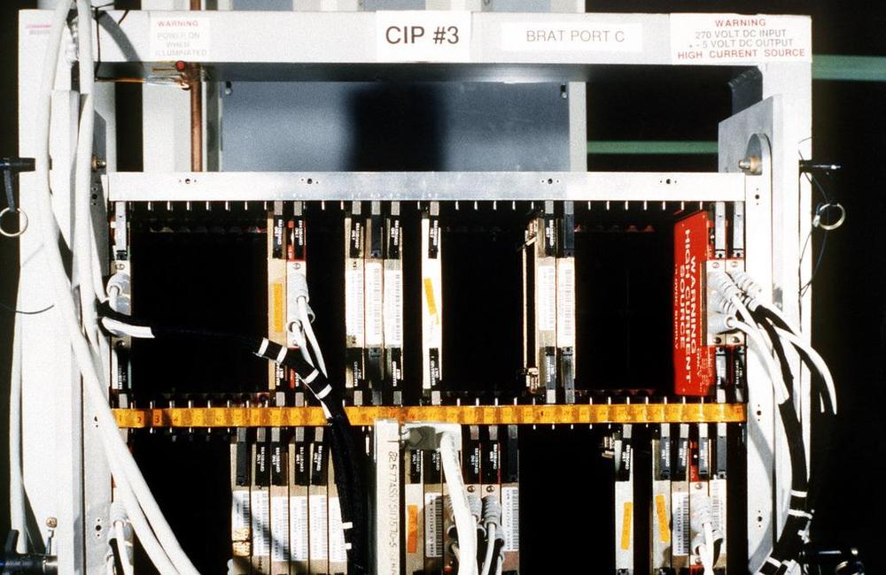
Hughes designed a modular avionics processor that used the i960 XA and later the MX. A dense module called the HAC-32 contained two i960 MX processors, 2 MB of RAM, and an I/O controller in a 2"×4" multi-chip module, slightly bigger than a credit card. This module had bare dies bonded to the substrate, maximizing the density. In the photo below, the two largest dies are the i960 MX while the numerous gray rectangles are memory chips. This module was used in F-22's Common Integrated Processor, the RAH-66 Comanche helicopter (which was canceled), the F/A-18's Stores Management Processor (the computer that controls attached weapons), and the AN/ALR-67 radar computer.
The military market is difficult due to the long timelines of military projects, unpredictable volumes, and the risk of cancellations. In the case of the F-22 fighter plane, the project started in 1985 when the Air Force sent out proposals for a new Advanced Tactical Fighter. Lockheed built a YF-22 prototype, first flying it in 1990. The Air Force selected the YF-22 over the competing YF-23 in 1991 and the project moved to full-scale development. During this time, at least three generations of processors became obsolete. In particular, the i960MX was out of production by the time the F-22 first flew in 1997. At one point, the military had to pay Intel $22 million to restart the i960 production line. In 2001, the Air Force started a switch to the PowerPC processor, and finally the plane entered military service in 2005. The F-22 illustrates how the fast-paced obsolescence of processors is a big problem for decades-long military projects.
The Common Integrated Processor for the F-22, presumably with i960 MX chips inside. It is the equivalent of two Cray supercomputers and was the world's most advanced, high-speed computer system for a fighter aircraft. Source: NARA/Hughes Aircraft Co./T.W. Goosman.
Intel charged thousands of dollars for each i960 MX and each F-22 contained a cluster of 35 i960 MX processors, so the military market was potentially lucrative. The Air Force originally planned to buy 750 planes, but cut this down to just 187, which must have been a blow to Intel. As for the Comanche helicopter, the Army planned to buy 1200 of them, but the program was canceled entirely after building two prototypes. The point is that the military market is risky and low volume even in the best circumstances.21 In 1998, Intel decided to leave the military business entirely, joining AMD and Motorola.
Foreign militaries also made use of the i960. In 2008 a businessman was sentenced to 35 months in prison for illegally exporting hundreds of i960 chips into India for use in the radar for the Tejas Light Combat Aircraft.
i960: the later years
By 1990, the i960 was selling well, but the landscape at Intel had changed. The 386 processor was enormously successful, due to the Compaq Deskpro 386 and other systems, leading to Intel's first billion-dollar quarter. The 8086 had started as a stopgap processor to fill a temporary marketing need, but now the x86 was Intel's moneymaking engine. As part of a reorganization, the i960 project was transferred to Chandler, Arizona. Much of the i960 team in Oregon moved to the newly-formed Pentium Pro team, while others ended up on the 486 DX2 processor. This wasn't the end of the i960, but the intensity had reduced.
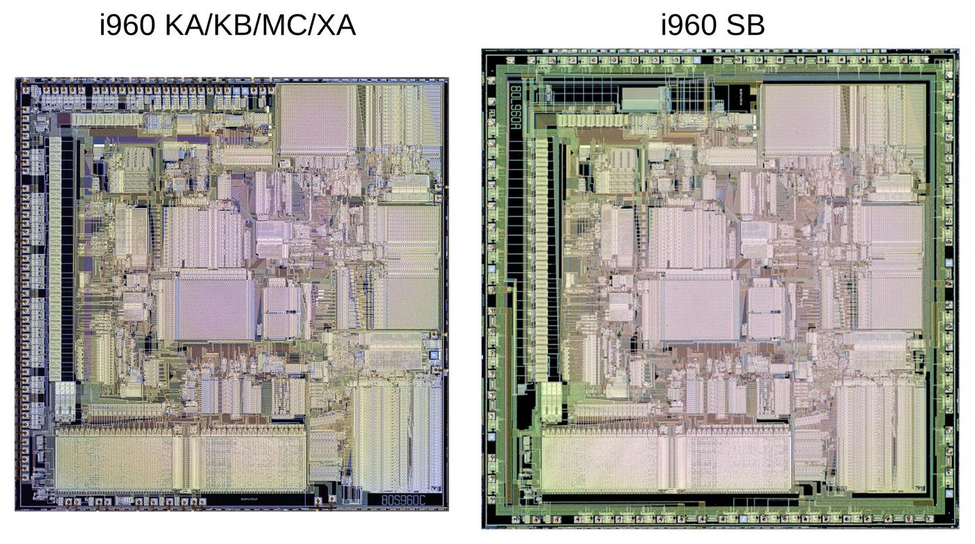
To reduce system cost, Intel produced versions of the i960 that had a 16-bit bus, although the processor was 32 bits internally. (This is the same approach that Intel used with the 8088 processor, a version of the 8086 processor with an 8-bit bus instead of 16.) The i960 SB had the "Numerics" architecture, that is, with a floating-point unit. Looking at the die below, we can see that the SB design is rather "lazy", simply the previous die (KA/KB/MC/XA) with a thin layer of circuitry around the border to implement the 16-bit bus. Even though the SB didn't support memory management or objects, Intel didn't remove that circuitry. The process was reportedly moved from 1.5 microns to 1 micron, shrinking the die to 270 mils square.
Comparison of the original i960 die and the i960 SB. Photos courtesy of Antoine Bercovici.
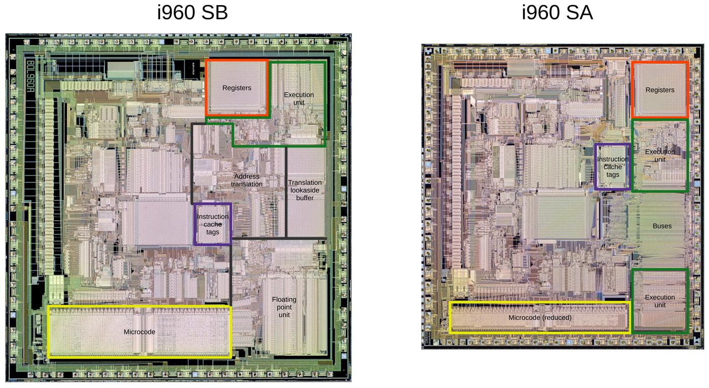
The next chip, the i960 SA, was the 16-bit-bus "Core" architecture, without floating point. The SA was based on the SB but Intel finally removed unused functionality from the die, making the die about 24% smaller. The diagram below shows how the address translation, translation lookaside buffer, and floating point unit were removed, along with much of the microcode (yellow). The instruction cache tags (purple), registers (orange), and execution unit (green) were moved to fit into the available space. The left half of the chip remained unchanged. The driver circuitry around the edges of the chip was also tightened up, saving a bit of space.
This diagram compares the SB and SA chips. Photos courtesy of Antoine Bercovici.
Intel introduced the high-performance Hx family around 1994. This family was superscalar like the CA/CF, but the Hx chips also had a faster clock, had much more cache, and included additional functionality such as timers and a guarded memory unit. The Jx family was introduced as the midrange, cost-effective line, faster and better than the original chips but not superscalar like the Hx. Intel attempted to move the i960 into the I/O controller market with the Rx family and the VH.23 This was part of Intel's Intelligent Input/Output specification (I2O), which was a failure overall.
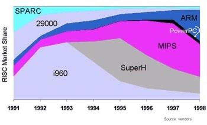
For a while, the i960 was a big success in the marketplace and was used in many products. Laser printers and graphical terminals were key applications, both taking advantage of the i960's high speed to move pixels. The i960 was the world's best-selling RISC chip in 1994. However, without focused development, the performance of the i960 fell behind the competition, and its market share rapidly dropped.
Market share of embedded RISC processors. From ExtremeTech.
By the late 1990s, the i960 was described with terms such as "aging", "venerable", and "medieval". In 1999, Microprocessor Report described the situation: "The i960 survived on cast-off semiconductor processes two to three generations old; the i960CA is still built in a 1.0-micron process (perhaps by little old ladies with X-Acto knives)."22
One of the strongest competitors was DEC's powerful StrongARM processor design, a descendant of the ARM chip. Even Intel's top-of-the-line i960HT fared pitifully against the StrongARM, with worse cost, performance, and power consumption. In 1997, DEC sued Intel, claiming that the Pentium infringed ten of DEC's patents. As part of the complex but mutually-beneficial 1997 settlement, Intel obtained rights to the StrongARM chip. As Intel turned its embedded focus from i960 to StrongARM, one writer wrote, "Things are looking somewhat bleak for Intel Corp's ten-year-old i960 processor." The i960 limped on for another decade until Intel officially ended production in 2007.
RISC or CISC?
The i960 challenges the definitions of RISC and CISC processors.24 It is generally considered a RISC processor, but its architect says "RISC techniques were used for high performance, CISC techniques for ease of use."25 John Mashey of MIPS described it as on the RISC/CISC border26 while Steve Furber (co-creator of ARM) wrote that it "includes many RISC ideas, but it is not a simple chip" with "many complex instructions which make recourse to microcode" and a design that "is more reminiscent of a complex, mainframe architecture than a simple, pipelined RISC." And they were talking about the i960 KB with the simple Numerics architecture, not the complicated Extended architecture!
Even the basic Core architecture has many non-RISC-like features. It has microcoded instructions that take multiple cycles (such as integer multiplication), numerous addressing modes27, and unnecessary instructions (e.g. AND NOT as well as NOT AND). It also has a large variety of datatypes, even more than the 432: integer (8, 16, 32, or 64 bit), ordinal (8, 16, 32, or 64 bit), decimal digits, bit fields, triple-word (96 bits), and quad-word (128 bits). The Numerics architecture adds floating-point reals (32, 64, or 80 bit) while the Protected architecture adds byte strings with decidedly CISC-like instructions to act on them.28
When you get to the Extended architecture with objects, process management, and interprocess communication instructions, the large instruction set seems obviously CISC.29 (The instruction set is essentially the same as 432 and the 432 is an extremely CISC processor.) You could argue that the i960 Core architecture is RISC and the Extended architecture is CISC, but the problem is that they are identical chips.
Of course, it doesn't really matter if the i960 is considered RISC, CISC, or CISC instructions running on a RISC core. But the i960 shows that RISC and CISC aren't as straightforward as they might seem.
Summary
The i960 chips can be confusing since there are four architectures, along with scalar vs. superscalar, and multiple families over time. I've made the table below to summarize the i960 family and the approximate dates. The upper entries are the scalar families while the lower entries are superscalar. The columns indicate the four architectural variants; although the i960 started with four variants, eventually Intel focused on only the Core. Note that each "x" family represents multiple chips.
| Core | Numerics | Protected | Extended | |
|---|---|---|---|---|
| KA | KB | MC | XA | Original (1988) |
| SA | SB | Entry level, 16-bit data bus (1991) | ||
| Jx | Midrange (1993-1998) | |||
| Rx,VH | I/O interface (1995-2001) | |||
| CA,CF | MM | MX | Superscalar (1989-1992) | |
| Hx | Superscalar, higher performance (1994) |
Although the i960 is now mostly forgotten, it was an innovative processor for the time. The first generation was Intel's first RISC chip, but pushed the boundary of RISC with many CISC-like features. The i960 XA literally set the standard for military computing, selected by the JIAWG as the military's architecture. The i960 CA provided a performance breakthrough with its superscalar architecture. But Moore's Law means that competitors can rapidly overtake a chip, and the i960 ended up as history.
Thanks to Glen Myers, Kevin Kahn, Steven McGeady, and others from Intel for answering my questions about the i960. Thanks to Prof. Paul Lubeck for obtaining documentation for me. I plan to write more, so follow me on Twitter @kenshirriff or RSS for updates. I've also started experimenting with Mastodon recently as @[email protected] and Bluesky as @righto.com so you can follow me there too.
