Introduction
In the last two decades, there has been tremendous progress in radio-frequency, millimeter-wave, and sub-terahertz integrated circuits and systems, demonstrating complex phased arrays and multi-input, multi-output (MIMO) arrays with chip-scale systems, enabling new applications in radar, autonomous driving, 5G, gesture recognition, localization and more. Design of these chips involves a series of complex iterative design processes constituting of co-design and optimization of integrated active circuit elements and passive electromagnetic (EM) structures1,2,3,4,5,6,7. Every circuit in the high-frequency path of RF/sub-THz integrated chips (such as low noise and variable gain amplifiers, mixers for frequency translation, filters, signal distribution networks, quadrature signal generation, power amplifiers) is a combination of active and passive circuits8. The passive structures include one-port structures such as antennas; two-port structures such as matching networks, filters; three-port structures such as diplexers, combiners, splitters, switches; four-port structures such as couplers for quadrature signal generation, baluns for differential signal generations; and higher order networks such as beamforming structures with lens-like properties. Design processes of these circuits, active and passive, radiative and non-radiative, single-port or multi-port, are quite distinct from each other as they have different pre-selected templates with regular geometries. These design approaches have historically relied on intuition-based standard templates with a finite set of parameters (Fig. 1a). These are subsequently optimized with time-consuming parameter sweeps, ad-hoc population-based meta heuristic optimization methods, or with machine-learning-based surrogate models9,10,11,12,13,14. The co-design process essentially aims to tailor the electromagnetic structures and the active circuit topologies to optimize the collective response of the end-to-end circuit. The complexity of the design space makes exhaustive optimization non-tenable.
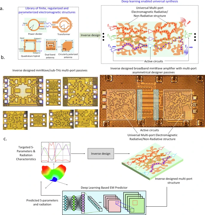
a The proposed approach for chip synthesis with inverse-designed arbitrary-shaped multi-port radiative and non-radiative structures co-designed with circuits. b Inverse-designed integrated multi-port millimeter-wave passive structures and end-to-end mm-Wave amplifier circuit chip with co-design between multi-port passive and active circuitry. The chips are fabricated in industry standard 90-nm BiCMOS foundry. c Inverse synthesis of arbitrary multi-port electromagnetic structures with desired scattering and radiating properties, enabled through a deep-learning based forward electromagnetic emulator. The latter takes the image of the structure and predicts accurately its multi-port scattering and radiating properties across frequencies in the space of arbitrary-shaped planar structures.
Currently, there exists no universal and generalized approach to synthesis for such complex high-frequency circuits. The bottom-up iterative design approaches with pre-fixed templates, hand-crafted designs, and ad-hoc parameter sweeps have several limitations. First, by choosing a template, we have already narrowed down the design and trade-off space. It is not clear at all that the end result could be close to being optimal in terms of efficiency, compactness, spectral range coverage, or other performance parameters. It can be noted that most of these designed structures are typically far from the fundamental limits (such as Bode-Fano) due to the losses associated with energy storage elements. Therefore, it is quite possible that an entire design space that lies outside the scope of these regular template-based geometries can yield significant improvement over traditional solutions. Second, the design process is time and resource intensive. Sometimes design is left to the domain expert, dominated by rules of thumb and trial-error. Otherwise, iterative optimization with complex electromagnetic simulations is needed. Moreover, classical approaches with machine-learning-based surrogates12,15, are only limited to one particular type of functional block with a pre-defined topology. Third, due to the nature of simplicity, these geometries have limited functionalities. For example, design of symmetrical power dividers with amplitude and phase equality operating at a given frequency is known with a rule-based approach. However, there are no set rules to engineer broader bandwidth or allowing unequal power division with spectrally-dependent phase relationship across frequencies. Nevertheless, as an example, for the same number of reactive elements, it has been shown that asymmetric circuits relax the trade-offs of classical symmetrical topologies, allowing higher efficiency operation over much broader bandwidths when combined with power amplifiers16,17,18. In this regard, new sub-THz/THz sensing and communication architectures emerge through such innovative design methods, that require new insights into particular applications18,19.
Here, we present a generalized approach for synthesis of arbitrary-shaped planar multi-port RF/sub-THz EM structures in minutes, with arbitrary scattering and radiative properties, integrated on-chip or realized off-chip in package. The approach to search this extensively large design space is made possible by deep-learning based forward modeling that allows us to eliminate time and resource intensive EM simulation runs, but is also robust enough to capture the complexities of scattering and radiating properties of arbitrary multi-port geometries. When co-designed with circuits, this can open up a path towards automated synthesis of end-to-end RF/sub-THz ICs, potentially achieving performance beyond the capabilities of state of the art template-based circuits.
Prior works in nanophotonics have demonstrated the class of inverse methods for specific dielectric-based passive structures through gradient based optimizations such as adjoint method20,21,22,23,24. In the photonics domain, the inverse-designed devices are mostly passive structures with standard waveguide interfaces that achieve a certain functionality with a tailored frequency response. The key difference in mm-Wave systems is the presence of active devices. Multiple active devices interact closely with passive structures, and also with each other to create functionalities such as impedance modulation, frequency synthesis, up/down-conversion, and so on. The complex impedances of these devices, their ability to amplify, and their mutual interactions need to be taken into account to realize an optimized end-to-end design process. Therefore, the passives are not designed separately as functional blocks, but collectively with the integrated devices—the latter may number from tens to tens of thousands depending on the complexity of circuits that are being realized, all of which can still be integrated on-chip. Second, the RF/sub-THz passive structures mostly support quasi-TEM modes with metal surfaces (realized in the back-end-of-the-line metal layers inside the chip) sandwiched within the chip dielectric. The losses per wavelength are much higher compared to photonics, and area minimization is a critically important consideration. Building robust model that captures the loss factors accurately, at the resolution of each pixel ( ~ λ/100) is also very challenging. When compared to low-frequency RF, on the other hand, it can be pointed out that at sub-THz and THz frequencies, the passives are small enough that they can be integrated on-chip directly with the active devices, allowing these complex systems to be fully integrated. These new opportunities as well as new challenges, can be addressed through AI-aided design tools. When compared to more restrictive cases in prior works12,13,15,25,26,27,28,29,30,31, this work presents a generalized method to explore the large design space of arbitrary multi-port EM structures and circuits, that allows curated functionalities and spectral properties.
To navigate the space of arbitrary-shaped multi-port RF/sub-THz EM structures and designer specified properties, we utilize a set of deep learning based models that predict accurately both scattering and radiative properties of arbitrary planar EM structures. This is a non-trivial exercise given that for an arbitrary pixelated structure, as represented in (Fig. 2a, b) with a 25 × 25 grid, the design space covers 2625 ≈ 10188 possible designs. Utilizing these models, we explore a generalized synthesis approach across several single and multi-port structures (including filters, resonators, power splitters, combiners, quadrature hybrids, diplexers, and antennas) and end-to-end mm-Wave circuits. This is the first step towards AI-enabled inverse design approach of complex RF/sub-THz circuits, which would open up a new design space by removing the constraints of template geometries, designer experience, trial and error, and ad-hoc optimization methods.

a Prediction of the scattering parameter of a single-port antenna structure (against a 3-D electromagnetic finite-element-method solver) embedded in a high-frequency dielectric between 20-40 GHz. b. Prediction of scattering parameters of two-port filter structures between 30-100 GHz realized with arbitrary transmission-line based and pixelated structures (16 × 16 pixel). The comparison against full 3-D EM simulation demonstrates the accuracy of the deep-learning model. c Prediction of antenna radiation patterns between 20-40 GHz demonstrates ability to predict both scattering and radiating properties, allowing generalization as depicted in Fig. 1a. d. Average prediction error of synthesis results for arbitrary-shaped three-port structures (25 × 25 pixels, 400 × 400 μm) at three representative frequencies between 24 and 80 GHz. A detailed snapshot of predicted and EM simulated scattering parameters of test set for both real and imaginary components of scattering parameters of the three port structures show strong correlation, indicating excellent prediction accuracy.
Results
Deep convolutional neural network as arbitrary scattering and radiative multi-port EM emulator
The conceptual EM emulator of the N-port arbitrary EM structure is represented in Fig. 1c. The input is the arbitrary geometry with arbitrary port placements, and the output is the predicted multi-port scattering and radiative properties, including complex S-parameters and radiation patterns. The relationship between the arbitrary planar geometry to the EM behavior is complex and nonlinear, and while multi layer perceptrons can act as a universal nonlinear mapper, simple application of such networks may result in overfitting due to the vastly under-sampled training data set. To this end, in order to justify the selection of convolutional neural networks, we rely on physics-based intuition. The effective scattering and radiating properties of these EM structures are effectively determined by the spatial distribution of electrical and magnetic near-fields and the boundary conditions. To capture these spatially distributed properties within the EM structure, several layers of convolutional filters of varying sizes, are applied to the image of the structure32. Since convolution operation is shift invariant, relative location of features are captured within the structure33,34. An example feature would be the distance between excitation ports and AC shorting locations. Even if ports are placed at different locations within the structure, sliding convolutional filters can still extract relative placement of other features. Such geometric properties of convolutional networks supplement their applicability to physics problems where structures with equivalent geometries are frequently encountered. In addition, through training, the network can learn to extract the relevant features, which is in contrast to classical machine learning tools where a set of pre-defined and pre-extracted features are utillized35. It should be noted that since deep-learning-based synthesis approach aims to move away from intuition-based parameterized designs, providing a set of pre-determined features would be counteracting this goal. To enable a widely generalizing model of such arbitrary structures, we pay close attention to the training dataset and optimal CNN architecture.
CNN architecture and technology portability
The goal here is to perform efficient training through the use of transfer learning which is applicable to multiple different scenarios such as different process nodes in chips, frequency sets, different dielectric stacks and packaging. Generalizability and model accuracy are key training targets to ensure robust inverse synthesis. Since we train different CNNs for distinct datasets (across process nodes, bounding box size, and pixel number), an architecture optimization would naturally give rise to different CNN hyper-parameters (Supplementary Material Table-1). Nevertheless, several general features have been adopted as a rule of thumb. It is generally accepted that deeper networks are more capable than wider ones32. In parallel to this, the first 10 to 15 layers of the CNN are convolutional layers with progressively reducing filter sizes. Each convolutional layer has 64 learnable filters followed by batch normalization (batch-norm) and leaky Rectified Linear Unit (ReLU)36,37. While batch-norm allows for smoother training for deep neural networks, leaky ReLU avoid vanishing gradients. The output of final convolutional layer is flattened and fed to fully connected (FC) layers. The number of FC layers are considerably less than convolutional layers (5–6). FC layers are followed by batch-norm, leaky ReLU, and dropout layers. During the training, dropout layers randomly shut down a fixed percentage of neurons, which mitigates overfitting38. Moreover, during these training runs, periodic validations (after each epoch) were performed to end the training early if the validation error is no longer improving. ADAM optimizer was used for conducting training runs39.
Here, we desire to limit real and imaginary part of predicted S-Parameters to the range of [-1,1], as we are considering passive structures. Even then, small numerical errors in the prediction results can violate passivity condition. After the prediction, passivity violations are corrected with minimum perturbations40. Finally, test set error and training set error was compared to ensure that generalization ability of the CNN is not impaired. The final architecture is then picked based on the test set error.
Since we are interested in integrated RF/sub-THz circuits, we train CNNs that predicts the spectral response of electromagnetic structures realized on-chip, across 24-100 GHz. This predictor model is the critical component that allows us to engineer EM structure spectral response (Fig. 2). To allow efficient training, we utilize transfer learning to optimize prediction accuracy by using a large number of inexpensive, low accuracy simulations as the initial training step41. This initial training result is then re-trained (or tuned) with a smaller number of higher accuracy simulations. The scalability of the model in predicting performance across varying bounding box sizes and frequency can also be ensured efficiently through transfer learning. In addition, we apply data augmentation using geometric transformations (such as flipping the EM structure upside down) to reduce required number of simulations30,42,43. Once the data has been generated, training takes a few hours (2–3 with contemporary GPUs), and inverse synthesis takes a few minutes starting from the desired parameters. More details about the datasets and training steps have been provided in Supplementary Material Tables 1–3.
Figure 2a, b and c demonstrate the the robustness of the deep learning models in predicting the scattering parameters of arbitrary planar multi-port EM structures across the broad range of frequencies, either integrated or realized on package, radiative and non-radiative. Once trained, the model accurately predicts the properties of a one-port classical corner cut antenna realized on off-chip package (12 × 12 pixels within 2.4 × 2.4 mm). The figures also shows accurate prediction of classical two-port filters realized with transmission lines with multiple stubs (16 × 16 pixels within 300 × 300 μm), and an on-chip randomly generated 3-port pixelated network (25 × 25 pixels within 400 × 400 μm). For antennas, the predicted radiation patterns also match closely to the EM simulations (Fig. 2c). Figure 2d shows the average prediction errors for three-port EM structures (25 × 25 pixels for 400 × 400 μm structures) across 24, 50, and 80 GHz demonstrating robust predictions. Here, prediction error was calculated as ∣s'-s∣ where s' is the predicted S-Parameter. Figure 2d also illustrates the scatter plot of the simulated and predicted S-parameters (real and imaginary) at the selected frequency of 50 GHz. For different scattering parameters terms, the heat map is tightly concentrated around the y = x diagonal, indicating good correlation between prediction and simulation results. These results show a remarkably low average error in prediction ability in the design space of arbitrary structures.
Generalized inverse synthesis
Utilizing the deep-learning enabled robust EM emulator that eliminates the need for time and resource intensive EM simulations, one can now conceive of rapid synthesis in the large design space of arbitrary structures and circuits with optimization algorithms (Fig. 1c). This can either be achieved through heuristic algorithms such as genetic algorithms (GA), simulated annealing or generative AI tools such as auto-encoders or tandem neural networks26. One can use the predictive model with a generative AI framework or with RL. We provide a more extensive comparison a the generative AI framework for synthesis in Supplementary Material Fig. S2.
Starting from a random structure, quick convergence to candidate solutions can be achieved through the evolution process. In this aspect, hyper-parameter choice for the GA is essential for ensuring exploratory strategy of the optimization loop. Firstly, we use a tournament selection method to determine the parents of each member of the next generation44. For a typical population size of M=4096, a tournament size of N=256 is adopted. As a result, population members with above average success have a decent chance for being selected as the parent. Upon parent selection and crossing over, each pixel has a mutation probability of flipping. This probability starts from 0.1 and vanishes to 0 towards the end of total number of iterations (100 in this paper). In addition, the best A=8 members of the current population are directly transferred to the next generation, guaranteeing a monotonous cost value reduction trajectory.
Figure 3 illustrates with several examples robust generalized inverse synthesis approach performed from single port antennas to multi-port EM structures based on the targeted scattering parameters; including one-port multi-band antennas, two-port bandpass filters, three-port power dividers with unique phase relationship, four-port resonant quadrature hybrid and three-port frequency diplexers. Figure 3a shows a packaged multi-band antenna (matched at 25 and 28 GHz) implemented in a compact area. In Fig. 3b, we show the synthesis of a band-pass two-port filter designed for 50-60 GHz, compressed to a size of λ/10 × λ/10 synthesized in a few minutes. For three ports, we demonstrate two complex design examples. In Fig. 3c, the input signal gets equally power split between two paths and maintain a 90∘ phase difference between the two paths at 60 GHz. The evolved EM structure achieves this almost exactly with nearly 0 dB amplitude difference, 1 dB insertion loss and 88∘ phase difference. In the second 3-port structure (Fig. 3e), we synthesize a diplexer that splits the single input into two paths depending on the frequency (similar to a wavelength division multiplexer). The lower band is 24–40 GHz and the upper band is 60–80 GHz. It can be seen that the method successfully achieves a diplexer with 2–4 dB insertion loss, and adjacent channel leakage less than -10 dB between 30-80 GHz, within an implemented area of λ/6 × λ/6 at the crossover frequency of 50 GHz. Figure 3d shows a 4-port EM structure with quadrature symmetry implementing a hybrid coupler.

a Inverse synthesis of multi-band packaged mm-Wave antenna operating at 24 and 28 GHz. b Inverse synthesis of a 2-port on-chip bandpass filter with a pass band target of 50-60 GHz. The filter (16 × 16 pixel, 300 × 300 μm) is compact with each side being λ/10 at 50 GHz. c Inverse synthesis of a 3-port equal power divider with ≈ 90∘ phase shift between 2 output ports at 60 GHz. d Inverse synthesis of a a 4-port 24 × 24 pixel quadrature hybrid between 70 and 80 GHz, showing close to ideal amplitude balance and phase relationship. e. Inverse synthesis of on-chip frequency diplexer (20 × 20 pixel 500 × 500 μm) with channel bandwidths of 24–40 GHz and 60–80 GHz.
We also demonstrate how the initial structure evolves to the final one to approach the desired performance. In Fig. 4a, we show how the frequency diplexer circuit evolves across optimization steps. The two frequency slices show the desirable performance where the signal flows to port 1 at 37 GHz (S31 = 1, S32 = 0), and it flips at 80 GHz (S31 = 0, S32 = 1). We can observe that initially most of the population is spread randomly, and as the generations evolve, the structures start to move towards the target points, finally leading to the structure that approaches the desired performance.

a Scatter plot showing the evolutionary progress of the frequency diplexer design progressing towards the ideal design point for 37 and 80 GHz. b, c Demonstration of generalized learning ability by the inverse synthesis method. We compare the inverse synthesis of two EM structures. The first one is an unequal power divider with a 4.7 dB power difference between the two output ports. The second one is an equal power divider with a bandpass filter response. In both cases, the synthesized structures (25 × 25 pixel 400 × 400 μm) demonstrate a better result than the best of the training data. This demonstrates the ability of the deep learning based model to generalize, and the inverse synthesis to successfully sample the design space.
Generalization ability of CNN
The EM emulator model needs to be able to predict structures that are not present in the dataset, such as those that can outperform structures present in the training data set. This is necessary for generalized inverse synthesis method. Figure 4 demonstrates this generalization ability as the inverse synthesis can tailor the structure to engineer the spectral response, distinctly different from what it has been trained with. The figure compares the results of structure that emerged through inverse synthesis and the best results from the training data for 2 different targets. Figure 4b shows the synthesis of a broadband uneven power divider that aims a power splitting ratio of 75%-25% across the bandwidth from 24 to 80 GHz. As it can be seen, the inverse design solution achieves better bandwidth, amplitude balance, and total transmission across 24-80 GHz, when compared to the best result from the training data. This demonstrates that the CNN model is not a lookup table, but is able to extract the relevant features that can robustly predict the scattering parameters of arbitrary structures, allowing the ability to search through this unexplored space during synthesis. Figure 4c shows a filtering power divider that performs equal power split and band pass filtering in each of the signal paths. Compared to the sample from the dataset, inverse design solution can provide a better trade-off between pass-band and stop-band requirements, while achieving near perfect amplitude and phase balance.
Furthermore, we can show that the initial computational cost for training dataset generation can be amortised very quickly by utilizing inverse design for different design goals. This was illustrated in detail in Fig. 5. When compared to the traditional EM simulation-based meta-heuristic methods, CNN aided inverse design can reduce design time to minutes from weeks, significantly reducing time and resource for synthesis. Moreover, once a model is trained it could be re-utilized for different design targets, which is in contrast to EM-based optimization where a new set of simulations needs to be performed at for different set of goals.
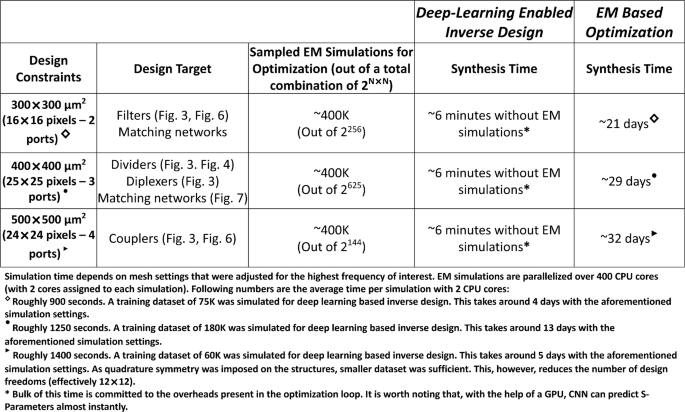
By removing the constraints of iterative EM simulations, the proposed method can drastically reduce the time of synthesis. Moreover, once a model trained, it can be utilized for different design goals and synthesize EM structures within minutes, which is in stark contrast with EM-based optimization.
Measurement results
To validate the generalized synthesis approach, we design, fabricate, and measure several examples of electromagnetic structures for mm-Wave frequencies, as well as an end-to-end broadband mm-Wave amplifier. All the electromagnetic structures and the mm-Wave amplifier are fabricated in industry standard bipolar complementary-oxide-metal-semiconductor (BiCMOS) process. The antennas are realized in a standard printed circuit board (PCB) process. We first present the results of two-port band-pass filter structures, and examine experimentally the effect of the size of the structure, number of pixels, and the results with different optimization algorithms, such as genetic algorithm (GA) and binary particle swam optimization (BPSO).
Size
The inverse synthesis can be guided to search for a compact structure that achieves a desired spectral response. Ultimately, this is limited by Maxwell’s laws. An electromagnetic structure effectively distributes electrical and magnetic energy within the structure to synthesize any spectral response. Therefore, the structure needs to be comparable to the wavelength to allow resonant-type behavior. Figure 6 captures this experimentally as we scale the structure from λ/12 × λ/12 (200 μm in each side) to λ/5 × λ/5 (500 μm in each side) across three step sizes, all implemented in the BiCMOS process. As can be seen in Fig. 6a, the spectral response can be seen to made broadband (covering 50-70 GHz) with flatter passband responses, due to more effective containment of the energy at 60 GHz with less leakage.

a Frequency response of two-port band-pass filters (16 × 16 pixel) with varying sizes including 200 × 200 (≈λ/13 each size), 300 × 300 (≈λ/8) and 500 × 500 μm (≈λ/5). Increasing the size increases the effective filter order resulting in broadband response as seen in the measurements. b Inverse-designed filters with varying pixel sizes between 10 × 10, 12 × 12, and 16 × 16 pixels. While we obtained similar performances, 16 × 16 pixel combination provides the best trade-off between pass-band and stop-band requirements. c Comparison of inverse-designed 80 GHz band-pass filters (200 × 200 μm, 16 × 16 pixels) synthesized with GA and BPSO. d Inverse-designed integrated 4-port quadrature hybrid measuring 500 × 500 μm (≈λ/4) and 20 × 20 pixels. e, f Inverse-designed compact edge feed mm-Wave antenna at 22 GHz, and dual band antenna working at 25 and 28 GHz.
Number of pixels
To approach the nearly arbitrary dimensions (that allow maximum design freedom), the number of pixels has to be increased. However, this creates a trade-off between the training time and achieved performance. Here, we fix the EM structure size and observe the cost minimization for different pixel combinations. A 300 × 300 μm area was divided into 10 × 10, 12 × 12, and 16 × 16 pixels and optimized for 50–70 GHz band-pass filter response, as shown at Fig. 6b. While in this example, all of the three levels of discretization produce generally similar spectral response, in other more complex circuits, it is understandable that the additional degrees of freedom achieved via larger number of pixels can provide better performance.
Synthesis algorithm
The Inverse synthesis approach that is presented here is best suited to discrete valued optimization algorithms. Figure 6c illustrates one such comparison for an 80 GHz band-pass filter with 200 × 200 μm area, synthesized through a GA and a BPSO algorithm. Due to the non-convexity of the space, the different spectral response can be expected as seen in the measurement results.
Multi-port structures
We present inverse synthesis of multi-port electromagnetic structure through a four-port quadrature hybrid realized on-chip. It is noteworthy that, by imposing quadrature symmetry on 4-port networks, a hybrid coupler can be designed by just satisfying ∣S21∣ = ∣S31∣ = 0.707 as exemplified in Fig. 6d. As can be seen in the figures, the hybrid demonstrates nearly equal power through the coupled and through ports (≈−4 dB) between 70–80 GHz. Details for this measurement are given in the Supplementary Material Fig. S5.
Antennas
We synthesize mm-Wave antennas with edge feed and probe feed configurations as shown in Fig. 6e, f. These antennas are realized with standard PCB manufacturing. Figure 6e is a highly compact antenna occupying an area of λ2/9, compared to a typical patch antenna area of λ2/4, resulting in a 2.25× smaller area. Figure 6f demonstrates a dual-band design operating at 25 and 28 GHz. In addition, antenna radiation patterns are characterized at resonance frequency for the dominant polarization.
Generalized multi-port inverse synthesis for co-design with millimeter-wave circuits
The examples we provided until this point assume standard 50Ω input and output impedance. However, for integrated RF/sub-THz circuits, when these multi-port structures are driven by active devices, the port impedances are frequency-dependent and complex valued. We present an example of a multi-stage broadband mm-Wave amplifier in 90-nm SiGe-based BiCMOS process that exploits the asymmetrical irregular 3-port structures (synthesized through the generalized inverse synthesis method). Figure 7a shows the schematic and overall principle of operation of the broadband mm-Wave amplifier. Unlike a traditional symmetrical amplifier, the input signal splits asymmetrically into two paths with a frequency-dependent non-zero phase difference. The signal in each branch passes through two stages of amplifier cells, and then combines in phase through a second 3-port asymmetrical structure. To compensate for the phase difference between the input paths ( + Φ), the output combiner is also designed to create an opposite phase relationship ( − Φ), such that the signals combine in phase optimally at the output. In Fig. 7b, it is shown that ideal driving phase difference for the output combiner between each branch is provided by the input splitter. Furthermore, the synthesis process aims to minimize the insertion loss and amplitude imbalances. Insertion loss at the output is between 0.7–1.2 dB across 24–40 GHz. In the same frequency range, input matching network shows 1.5-4 dB insertion loss with an amplitude imbalance less than 1.3 dB (details in Supplementary Material Fig. S9). Lastly, since the ports are not isolated, active elements do interact with each other. This frequency-dependent interaction is the key to broadband impedance synthesis. As a result, amplifier cells at stage-2 are provided with optimal impedances for high gain.

a A broadband mm-Wave amplifier architecture that relies on asymmetrical power division at the input, and phase compensating combiner to create broadband frequency response. The three-port input and output combiners are synthesized through inverse design, and they are co-designed with multi-stage integrated active circuit amplifiers (that have complex terminating impedances). b The input signal splits into two asymmetrical paths, gets amplified through multiple stages, and recombines at the output with approximately same total phases in both paths. Simulated output combiner loss, ideal driving phases (−Φ) and input phase path (+Φ) showing near-ideal combination of the signal at the output. c Chip micrograph (750 × 1500 μm) showing the fabricated chip in an industry-standard 90-nm BiCMOS process. d Measured small signal response of the chip shows 3 dB bandwidth of 23.6-37.3 GHz with peak gain of ≈ 17.5 dB, owing to the asymmetrical networks synthesized through the inverse design approach.
Figure 7-c show the the die photo of the inverse-designed asymmetrical two-stage mm-Wave amplifier. Figure 7d shows measured and simulated S-parameters. A measured gain of 17.5–14.5 dB is obtained between 23.6 and 37.3 GHz, which covers most of the commercial 5G bands. The asymmetrical paths through the inverse-designed divider and combiner are shown in the figure. The RF short location of the output combiner provides the VCC connection via a bypass capacitor array. As is evident, the inverse synthesis approach allows us to explore this class of complex structures with the tailored scattering parameters necessary for the circuit functionality. Going beyond the traditional matching networks, the proposed method provides access to a new class of complex multi-port electromagnetic structures. Co-designing these EM structures with the circuits can allow untapped performance metrics and functionalities.
Discussion
Here, we present a generalized multi-port inverse design method for synthesis of complex integrated electromagnetic structures co-designed with RF/sub-THz circuits. This approach that captures both radiative and non-radiative behavior, and multiple ports that can be excited or tapped with active devices, varying excitations, and boundary conditions, is critical for tapping a new design space of arbitrary geometric structures and circuits. This is a significant advancement to inverse synthesis of passive or simple two-port structures. This is enabled through a deep-learning based forward model that acts as a robust and accurate predictor of scattering parameters of arbitrary structures, thereby eliminating time and resource intensive EM simulations for inverse synthesis. Furthermore, we illustrate that the forward model can demonstrate generalization and learning ability. The transfer learning approach allows quick portability to different dielectric stacks, bounding box size or frequency range.
We discuss the trade-off space, present several design examples, and report measurement results of fabricated antennas, filters, multi-port structures, and circuits. The generalized approach allows amortization of the simulation and training time across many designed circuits, while not being constrained to particular narrow design sets. Once trained, the synthesis achieves the target specifications within minutes. We believe that this approach not only opens up a new design space with previously unachievable performance, but also provides a path towards rapid and automated synthesis of complex RF/sub-THz circuits and systems; moving it beyond trial and error techniques, constraints of designer insights, and time and resource intensive iterative design methodologies. The multi-port generalization is the key to unleashing the universality of the design approach for rapid synthesis of complex RF/sub-THz wireless chip-scale systems at low cost.
Methods
Training process
Training datasets for inverse design were obtained through Matlab EM Toolbox, and we have used ANSYS HFSS (commercially available 3-D finite-element method electromagnetic solver) for design verification. Detailed overview of the training datasets are available in the Supplementary Material Tables 1–3. Matlab Deep Learning Toolbox was used for training and inference. It is possible to import the trained network to Python environment as well.
Design validation, fabrication, and measurement
Chips are fabricated using a 90-nm BiCMOS process. Relevant parts of the chip are shown in Figs. 6 and 7. Circuit details for the mm-Wave amplifier can be found in Fig. 7 and Supplementary Material Fig. S9. Verifications of inverse synthesis results were carried out via HFSS (Figs. 3, 4, 6, and 7b). For the example amplifier circuit, a full die EM simulation was performed with EMX (Fig. 7d).
On-wafer S-Parameter measurements are carried out with 67 GHz Anritsu VNA (with 110 GHz extension modules) using 110 GHz and 67 GHz GSG probes (Infinity and Z-Probe respectively). VNA calibrations were performed with calibration substrates of individual probe pairs. Antenna impedances were measured in a similar manner, albeit with a coaxial cable compatible calibration kit. Antenna radiation pattern verification were performed through over the air far field measurement using a 2-axis rotational hardware (details can be found in Supplementary Material Fig. S7). For the multi-port measurement of quadrature coupler, 50Ω on chip termination loads were de-embedded, as detailed in Supplementary Material Fig. S5.
Data availability
The training data for the algorithm is proprietary since it is trained on the process design kit of Global Foundries 9HP BiCMOS process (which is proprietary). The measurement data is available upon request.
Code availability
The code utilizes data that is proprietary to the process design kit of Global Foundries 9HP BiCMOS process (which is proprietary).
References
Ma, J. et al. Security and eavesdropping in terahertz wireless links. Nature 563, 89–93 (2018).
Ghasempour, Y., Shrestha, R., Charous, A., Knightly, E. & Mittleman, D. M. Single-shot link discovery for terahertz wireless networks. Nat. Commun. 11, 2017 (2020).
Sengupta, K., Nagatsuma, T. & Mittleman, D. M. Terahertz integrated electronic and hybrid electronic–photonic systems. Nat. Electron. 1, 622–635 (2018).
Venkatesh, S., Lu, X., Saeidi, H. & Sengupta, K. A high-speed programmable and scalable terahertz holographic metasurface based on tiled cmos chips. Nat. Electron. 3, 785–793 (2020).
Venkatesh, S., Lu, X., Tang, B. & Sengupta, K. Secure space–time-modulated millimetre-wave wireless links that are resilient to distributed eavesdropper attacks. Nat. Electron. 4, 827–836 (2021).
Monnai, Y., Lu, X. & Sengupta, K. Terahertz beam steering: from fundamentals to applications. J. Infrared, Millim., Terahertz Waves 44, 169–211 (2023).
Wu, X., Lu, H. & Sengupta, K. Programmable terahertz chip-scale sensing interface with direct digital reconfiguration at sub-wavelength scales. Nat. Commun. 10, 2722 (2019).
Shahramian, S., Holyoak, M. & Baeyens, Y. A 16-element w-band phased-array transceiver chipset with flip-chip pcb integrated antennas for multi-gigabit wireless data links. IEEE Trans. Microw. Theory Tech. 66, 3389–3402 (2018).
Nguyen, H. T. & Peterson, A. F. Machine learning for automating the design of millimeter-wave baluns. IEEE Trans. Circuits Syst. I Regul. Pap. 68, 2329–2340 (2021).
Munzer, D. et al. “Residual Network Based Direct Synthesis of EM Structures: A Study on One-to-One Transformers,” in 2020 IEEE Radio Frequency Integrated Circuits Symposium (RFIC), 143–146 (Los Angeles, CA, USA, 2020), https://doi.org/10.1109/RFIC49505.2020.9218278.
Nguyen, H. T. & Peterson, A. F. Machine learning for automating millimeter-wave directional coupler designs. IEEE Trans. Circuits Syst. II: Express Briefs 69, 549–553 (2022).
Liu, B., Zhao, D., Reynaert, P. & Gielen, G. G. E. Synthesis of integrated passive components for high-frequency rf ics based on evolutionary computation and machine learning techniques. IEEE Trans. Comput.-Aided Des. Integr. Circuits Syst. 30, 1458–1468 (2011).
Yu, H., Torun, H. M., Rehman, M. U. & Swaminathan, M. Design of siw filters in d-band using invertible neural nets. In 2020 IEEE/MTT-S International Microwave Symposium (IMS), 72–75 (2020).
Koziel, S., Pietrenko-Dabrowska, A. & Plotka, P. Reduced-cost microwave design closure by multi-resolution em simulations and knowledge-based model management. IEEE Access 9, 116326–116337 (2021).
Passos, F. et al. Pacosyt: A passive component synthesis tool based on machine learning and tailored modeling strategies towards optimal rf and mm-wave circuit designs. IEEE J. Microw. 3, 599–613 (2023).
Chappidi, C. R., Lu, X., Wu, X. & Sengupta, K. Antenna preprocessing and element-pattern shaping for multi-band mmwave arrays: Multi-port transmitters and antennas. IEEE J. Solid-State Circuits 55, 1441–1454 (2020).
Lu, X., Chappidi, C. R., Wu, X. & Sengupta, K. Antenna preprocessing and element-pattern shaping for multi-band mmwave arrays: Multi-port receivers and antennas. IEEE J. Solid-State Circuits 55, 1455–1470 (2020).
Chappidi, C. R., Sharma, T. & Sengupta, K. Multi-port active load pulling for mm-wave 5g power amplifiers: Bandwidth, back-off efficiency, and vswr tolerance. IEEE Trans. Microw. Theory Tech. 68, 2998–3016 (2020).
Wu, X. & Sengupta, K. On-chip thz spectroscope exploiting electromagnetic scattering with multi-port antenna. IEEE J. Solid-State Circuits 51, 3049–3062 (2016).
Molesky, S. et al. Inverse design in nanophotonics. Nat. Photon. 12, 659–670 (2018).
Liu, D., Tan, Y., Khoram, E. & Yu, Z. Training deep neural networks for the inverse design of nanophotonic structures. ACS Photon. 5, 1365–1369 (2018).
So, S., Badloe, T., Noh, J., Bravo-Abad, J. & Rho, J. Deep learning enabled inverse design in nanophotonics. Nanophotonics 9, 1041–1057 (2020).
Ma, W. et al. Deep learning for the design of photonic structures. Nat. Photon. 15, 77–90 (2021).
Hughes, T. W., Minkov, M., Williamson, I. A. & Fan, S. Adjoint method and inverse design for nonlinear nanophotonic devices. ACS Photon. 5, 4781–4787 (2018).
Karahan, E. A., Gupta, A., Khankhoje, U. K. & Sengupta, K. Deep learning based modeling and inverse design for arbitrary planar antenna structures at rf and millimeter-wave. In 2022 IEEE International Symposium on Antennas and Propagation and USNC-URSI Radio Science Meeting (AP-S/URSI), 499–500 (2022).
Gupta, A., Karahan, E. A., Bhat, C., Sengupta, K. & Khankhoje, U. K. Tandem neural network based design of multiband antennas. IEEE Trans. Antennas Propag. 71, 6308–6317 (2023).
Kim, Y., Keely, S., Ghosh, J. & Ling, H. Application of artificial neural networks to broadband antenna design based on a parametric frequency model. IEEE Trans. Antennas Propag. 55, 669–674 (2007).
Liu, B. et al. An efficient method for antenna design optimization based on evolutionary computation and machine learning techniques. IEEE Trans. antennas Propag. 62, 7–18 (2013).
Xiao, L.-Y., Shao, W., Jin, F.-L., Wang, B.-Z. & Liu, Q. H. “Inverse Artificial Neural Network for Multiobjective Antenna Design,” in IEEE Transactions on Antennas and Propagation, vol. 69, 6651–6659 (2021), https://doi.org/10.1109/TAP.2021.3069543.
Karahan, E. A., Liu, Z. & Sengupta, K. Deep-learning-based inverse-designed millimeter-wave passives and power amplifiers. IEEE J. Solid-State Circuits 58, 3074–3088 (2023).
Karahan, E. A., Liu, Z. & Sengupta, K. Ims deep learning enabled generalized synthesis of multi-port electromagnetic structures and circuits for mmwave power amplifiers. In 2024 IEEE/MTT-S International Microwave Symposium-IMS 2024, 184-187 (IEEE, 2024).
Goodfellow, I., Bengio, Y. & Courville, A.Deep Learning (MIT Press, 2016).
Saha, S. & Gokhale, T. Improving Shift Invariance In Convolutional Neural Networks With Translation Invariant Polyphase Sampling https://arxiv.org/abs/2404.07410 (2024).
Islam, M. A., Jia, S. & Bruce, N. D. B. How Much Position Information Do Convolutional Neural Networks Encode? https://arxiv.org/abs/2001.08248 (2020).
Li, Z., Liu, F., Yang, W., Peng, S. & Zhou, J. A survey of convolutional neural networks: Analysis, applications, and prospects. IEEE Trans. Neural Netw. Learn. Syst. 33, 6999–7019 (2022).
Ioffe, S. & Szegedy, C. Batch normalization: accelerating deep network training by reducing internal covariate shift. arXiv https://doi.org/10.48550/arXiv.1502.03167 (2015).
Maas, A. L. Rectifier Nonlinearities Improve Neural Network Acoustic Models https://api.semanticscholar.org/CorpusID:16489696 (2013).
Srivastava, N., Hinton, G., Krizhevsky, A., Sutskever, I. & Salakhutdinov, R. Dropout: a simple way to prevent neural networks from overfitting. J. Mach. Learn. Res. 15, 1929–1958 (2014).
Kingma, D. P. & Ba, J. Adam: A method for stochastic optimization. arXiv preprint arXiv:1412.6980 (2014).
Enforce passivity of rationalfit output or a rational object - matlab. https://www.mathworks.com/help/rf/ref/rfmodel.rational.makepassive.html.
Tan, C. et al. A Survey On Deep Transfer Learning (2018).
Liu, Z., Karahan, E. A. & Sengupta, K. Deep learning-enabled inverse design of 30-94 ghz psat,3db sige pa supporting concurrent multiband operation at multi-gb/s. IEEE Microw. Wirel. Compon. Lett. 32, 724–727 (2022).
Yang, S. et al. Image Data Augmentation For Deep Learning: A Survey (2023).
Goldberg, D. E. & Deb, K. Foundations Of Genetic Algorithms. Vol. 1, p. 69–93 (Elsevier, 1991).
Acknowledgements
The authors would like to acknowledge GlobalFoundries for chip fabrication support, and the following funding agencies: Army Research Office (W911NF2110314, K.S.), Air Force Office of Scientific Research (FA9550-23-1-0176, K.S.), Office of Naval Research (N00014-23-1-2592, K.S.), DURIP fundings (FA9550-22-1-0455, N00014-22-1-2302, K.S.), National Science Foundation (CNS-2211617, CNS-2148271, K.S.), and M. S. Chadha Center for Global India at Princeton University (K.S.). Authors express their gratitude to Suresh Venkatesh for his contributions to antenna manufacturing and measurement. Authors are thankful to Bert Harrop of Princeton Physics Department for his help with the chip packaging. The authors are pleased to acknowledge that the work reported on in this paper was substantially performed using the Princeton Research Computing resources. We acknowledge all our group members for technical discussions.
Ethics declarations
Competing interests
Authors have filed a United States provisional patent application on 17 June 2024, #63/660,874, entitled “Deep Learning Enabled Generalized Synthesis of Multi-Port Electromagnetic Structures and Circuits for Radio-Frequency Systems.”
Peer review
Peer review information
Nature Communications thanks Zongfu Yu and the other anonymous reviewer(s) for their contribution to the peer review of this work. A peer review file is available.
Additional information
Publisher’s note Springer Nature remains neutral with regard to jurisdictional claims in published maps and institutional affiliations.
Supplementary information
Rights and permissions
Open Access This article is licensed under a Creative Commons Attribution-NonCommercial-NoDerivatives 4.0 International License, which permits any non-commercial use, sharing, distribution and reproduction in any medium or format, as long as you give appropriate credit to the original author(s) and the source, provide a link to the Creative Commons licence, and indicate if you modified the licensed material. You do not have permission under this licence to share adapted material derived from this article or parts of it. The images or other third party material in this article are included in the article’s Creative Commons licence, unless indicated otherwise in a credit line to the material. If material is not included in the article’s Creative Commons licence and your intended use is not permitted by statutory regulation or exceeds the permitted use, you will need to obtain permission directly from the copyright holder. To view a copy of this licence, visit http://creativecommons.org/licenses/by-nc-nd/4.0/.
About this article

Cite this article
Karahan, E.A., Liu, Z., Gupta, A. et al. Deep-learning enabled generalized inverse design of multi-port radio-frequency and sub-terahertz passives and integrated circuits. Nat Commun 15, 10734 (2024). https://doi.org/10.1038/s41467-024-54178-1
Received:
Accepted:
Published:
Version of record:
DOI: https://doi.org/10.1038/s41467-024-54178-1