The shift to 3D ICs and chiplets demands automated, hierarchical design planning to manage exploding pin counts. Learn how Siemens EDA's Innovator3D IC addresses these challenges.
The semiconductor industry is undergoing a profound transformation, marked by a critical shift towards 3D IC technology. This evolution is not merely an incremental improvement but a fundamental necessity for the future of electronic systems. Driven by the relentless demand for higher performance, greater functionality, and more cost-effective solutions, the complexity of IC packaging has accelerated at an unprecedented rate.
This new era of integration presents both immense opportunities and significant challenges, pushing the boundaries of traditional design methodologies and demanding innovative approaches to managing the intricate web of connections within modern electronic devices. As we move further into the age of advanced packaging, understanding and addressing this escalating complexity becomes paramount for success in the rapidly evolving semiconductor landscape.
The industry stands at a pivotal juncture, where embracing 3D IC technology is no longer an option but a critical imperative for continued innovation and competitiveness.
Critical Shift to 3D ICs and Exponential Complexity
The traditional approaches to IC packaging design, which often relied on manual methods and generic tools like spreadsheets, are rapidly becoming obsolete in the face of modern complexity. While these tools might have sufficed for simpler, monolithic designs, they are inadequate for the multi-chiplet, multi-interposer assemblies prevalent today.
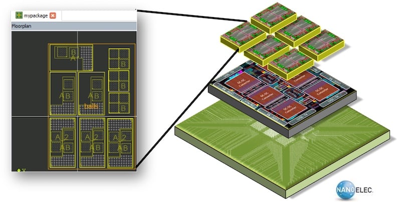
Arrayed blocks are used to construct a chiplet.
The sheer volume of data and the exponential growth in the number of connections within a package have rendered manual synchronization and management of co-designed components an insurmountable challenge. We have witnessed package pin counts explode from hundreds of thousands to tens of millions, with projections indicating a potential tenfold increase in the coming years.
This overwhelming complexity means that human oversight alone is no longer sufficient. The inability to manage vast amounts of data and interconnections manually introduces significant risks, leading to potential design flaws that can have catastrophic financial and operational consequences.
Traditional Methods Crumble Under Pin Count Explosion
The risks associated with these traditional, manual methods are substantial. A single error in a complex package design can lead to costly re-spins, significant delays in product launches, and even complete project failures. The financial implications alone can be devastating, given the immense investment required in semiconductor manufacturing.
Moreover, the increasing integration of diverse functionalities within a single package means that design flaws can propagate across multiple systems, leading to widespread performance issues or even safety concerns. The industry's reliance on outdated methods is a direct pathway to errors and delays, making a fundamental shift in design methodology an urgent requirement.
The sheer volume of data and interconnections far exceeds what any individual or team can manually manage, necessitating a fundamental shift in design methodology towards automated and abstract approaches that can break down complexity into manageable portions.
A key enabler in this new era of semiconductor design is the emergence of chiplets. These smaller, standardized building blocks offer a cost-effective alternative to monolithic system-on-chip (SoC) designs, facilitating easier integration and communication through standard interfaces such as UCI Express, BOW, and AIS.
By breaking down large designs into more manageable, reusable components, chiplets promise greater flexibility, faster time-to-market, and improved yield. This modularity allows for the creation of highly customized and optimized systems by combining various specialized chiplets, leading to more efficient and powerful electronic devices. Chiplets are emerging as a key enabler, providing a cost-effective alternative to monolithic SoCs.
Chiplets: Modular Advantage and Integration Challenge
However, this modularity comes with its own set of challenges, particularly in managing the explosion of interconnections and ensuring seamless integration across multiple disparate dies. The very advantage of chiplets – their ability to enable highly complex, heterogeneous integration – also contributes to the escalating complexity of the overall package.
Modern packages often involve multiple chiplets, interposers, and silicon bridges, many of which are being designed concurrently. Keeping all these elements in sync and managing the vast amounts of data manually is an exponential challenge, making the risk of errors multiply significantly, especially when considering the need for full 3D verification of these stacked designs.
The intricate interplay between different chiplets, each with its unique characteristics and requirements, demands a level of coordination and precision that far surpasses what traditional design flows can offer.
Given the overwhelming complexity now inherent in IC packaging, a fundamental shift towards automated and abstract approaches is essential to break down complexity into manageable portions. The core solution lies in working with abstraction levels, a concept central to hierarchical device planning.
This methodology allows designers to manage the intricate details of chiplet and interposer bump patterns without being overwhelmed by the individual pin-level complexity. While designing viable bump patterns for hundreds of thousands of pins was challenging but feasible in the past, dealing with millions or tens of millions of pins is simply impossible without advanced tools and a hierarchical approach.
Hierarchical Device Planning: Abstraction as the Solution
Hierarchical device planning enables designers to work at a higher level of abstraction, automating the process of implementing design changes and ensuring consistency across the entire system. This approach not only mitigates the risks associated with manual errors but also significantly improves design efficiency and accelerates the overall development cycle, allowing engineers to focus on higher-level architectural decisions rather than getting bogged down in minute details.
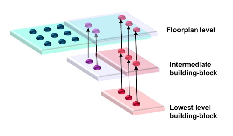
Connectivity in a hierarchical IC package floorplan, showing that bumps within the sub-devices are represented at the top level.
By abstracting away the lower-level complexities, designers can focus on critical aspects such as connectivity, power delivery, and thermal management at a system level, ensuring optimal performance and reliability. This methodology is indispensable for managing the explosion in design complexity, mitigating significant risks, and ensuring the successful realization of next-generation electronic systems.
To navigate the complexities and mitigate the risks inherent in modern IC packaging, designers require sophisticated tools that go far beyond traditional capabilities. These tools must not only manage complexity but also empower designers with insights and automation at every stage of the process.
The focus shifts from merely drawing connections to enabling intelligent planning, analysis, and verification. Addressing these multifaceted challenges, Siemens EDA introduced its Innovator3D IC portfolio solution.
This comprehensive suite covers the entire design flow, from initial planning and optimization through detailed analysis, package layout, and crucial work-in-progress (WIP) data management. The sheer volume of data involved in modern package designs necessitates robust version control and tracking to prevent errors caused by outdated or incorrect files.
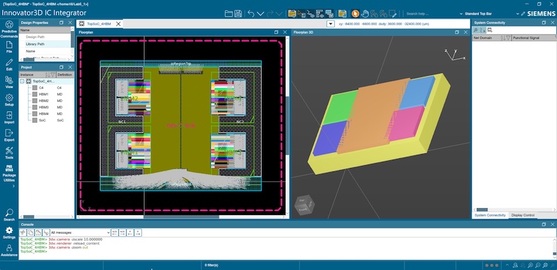
Innovator3D IC solution suite cockpit
A Comprehensive Platform for Next-Generation Design
The Siemens EDA Innovator3D IC portfolio provides the necessary capabilities to manage the unprecedented scale of integration and pin counts that define the future of chiplet ecosystems, ensuring that designers have the proper methodology and tools for the job. This solution empowers designers with a comprehensive suite of capabilities, including:
- Early Planning and Optimization: Tools for initial architectural exploration and optimization, allowing designers to make informed decisions early in the design cycle.
- Detailed Analysis: Advanced analysis capabilities for signal integrity, power integrity, and thermal analysis, ensuring robust and reliable performance.
- Package Layout: Intuitive and powerful tools for efficient and accurate package layout, accommodating the complexities of multi-chiplet and 3D stacked designs.
- Work-in-Progress (WIP) Data Management: Robust version control and tracking systems to manage vast amounts of design data, preventing errors and facilitating collaboration across distributed teams.
By integrating these functionalities into a cohesive platform, the Innovator3D IC portfolio streamlines the design process, reduces design cycles, and significantly lowers the risk of costly errors. It represents a critical advancement in design automation, providing the essential support needed for the next generation of electronic systems.
The journey through the complexities of modern IC packaging underscores a clear and urgent message: the industry must embrace new methodologies and advanced tools to succeed. While the challenges posed by accelerating complexity, chiplet integration, and exploding pin counts may seem daunting, effective solutions are available. The future of semiconductor design, characterized by advanced 3D ICs and chiplet integration, demands a proactive approach to adopting sophisticated design automation.
By leveraging hierarchical device planning, comprehensive analysis tools, and robust data management solutions like the Siemens EDA Innovator3D IC portfolio, companies can effectively navigate the increasing complexity, mitigate significant risks, and accelerate the development of next-generation electronic systems.
The solutions are indeed out there, waiting to be embraced by those willing to adapt their design processes and invest in the tools that define the cutting edge of semiconductor innovation. The transition to 3D IC technology is not merely a technological upgrade but a strategic imperative that will shape the future of electronics.
By embracing these advancements, the semiconductor industry can unlock new levels of performance, efficiency, and functionality, paving the way for groundbreaking innovations across diverse applications, from artificial intelligence and high-performance computing to automotive and consumer electronics.
All images used courtesy of Siemens EDA.