LLM inference is memory-bound. this means that most of the time is spent moving data, not doing the math.
so take the obvious extreme: make the chip big enough that you don’t have to move data (most of the time).
the NSA, NASA, and well-funded Silicon Valley startups in the 90s all tried. the technical problems were too deep and they failed.
Cerebras is the first to make this work. here i ignore if the business is viable and instead focus on the technology itself. the reason i did this research was because i was trying to answer the following questions for myself:
what does “make the chip bigger” actually buy you in terms of bandwidth and utilization?
why did wafer-scale computing fail historically?
what are the concrete failure modes?
why were those constraints considered unsolvable by smart people?
what did Cerebras do differently to make this viable?
how does the architecture actually work?
how do you program something like this in practice?
what are the remaining bottlenecks (I/O, prefill, throughput at scale, SRAM limits)?
this post is my effort to answer these questions from deep research & first principles.
every operation on a chip has two costs: doing the math, and getting the data to where the math happens. which one takes longer determines what you’re waiting on. if you wait on the data to move, you call that memory bottleneck. if you wait for the math to happen, you call it compute bottleneck.
the ratio between these two (memory v.s. compute bottlenecks) is called arithmetic intensity: FLOPs per byte moved from memory. every chip has a crossover point (the “ridge point”) where the two are equal:
ridge point = peak FLOPS / peak memory bandwidth
below the ridge point, you’re waiting on memory. the compute sits idle. above it, you’re waiting on math. you want to be above it.
a great resource to learn more about this is Modal’s GPU glossary section on the Roofline Model.
H100 in FP16: 989 TFLOPS peak, 3.35 TB/s bandwidth, ridge point = 295 FLOP/byte. so a workload needs 295 operations per byte of data to actually use the tensor cores.
LLM inference has two phases. prefill processes your whole prompt at once: matrix times matrix, and lots of data reuse. arithmetic intensity for a 512-token prompt on llama 70B works out to about 455 FLOP/byte. it’s above the ridge point, so it is compute-bound, and the GPU is busy. good.
decode generates tokens one at a time. the model reads all 140 GB of weights (70B params x 2 bytes at FP16), multiplies them against one vector, and produces one token. 140 GFLOP of math on 140 GB of data. arithmetic intensity is 1 FLOP/byte. the ridge point is 295, and you’re at 1. so the tensor cores are 99.7% idle.
tokens per second at this point is just bandwidth divided by model size: 3,350 GB/s / 140 GB = about 24 tok/s. the compute on the chip doesn’t matter here, because you could have 10x the tensor cores and it wouldn’t change anything. your bottleneck is moving the data to the correct place
this problem gets worse each GPU generation. this is generally referred to as the memory wall. the V100 had a 139x gap between decode intensity and ridge point. the H100: 295x. the B200: 563x. FLOPS simply grow faster than bandwidth.
if you process B users at once, you read the weights once and multiply against B vectors instead of 1. arithmetic intensity becomes roughly B. at batch 295 on an H100, you could finally be compute-bound!
the problem is that batch 295 for a 70B model needs KV cache for 295 simultaneous conversations, which would come to about 2 TB. but a single H100 has 80 GB, so you can’t even fit the model weights at FP16, let alone 295 conversations.
so GPU serving stacks (vLLM, TensorRT-LLM) use continuous batching to keep batch sizes as high as memory allows, usually 32-128 for large models. this gets utilization to maybe 10-40%. better than batch 1, but still not great. and every user you add to the batch makes each user’s tokens come out slower.
instead of amortizing weight reads across users, what if you make the memory so fast that even one user’s decode is efficient. SRAM delivers bandwidth proportional to how much you have, because every bank can be read simultaneously by the compute right next to it. an H100 has about 50 MB of SRAM, which not enough to store model weights.
unless you use the whole wafer.
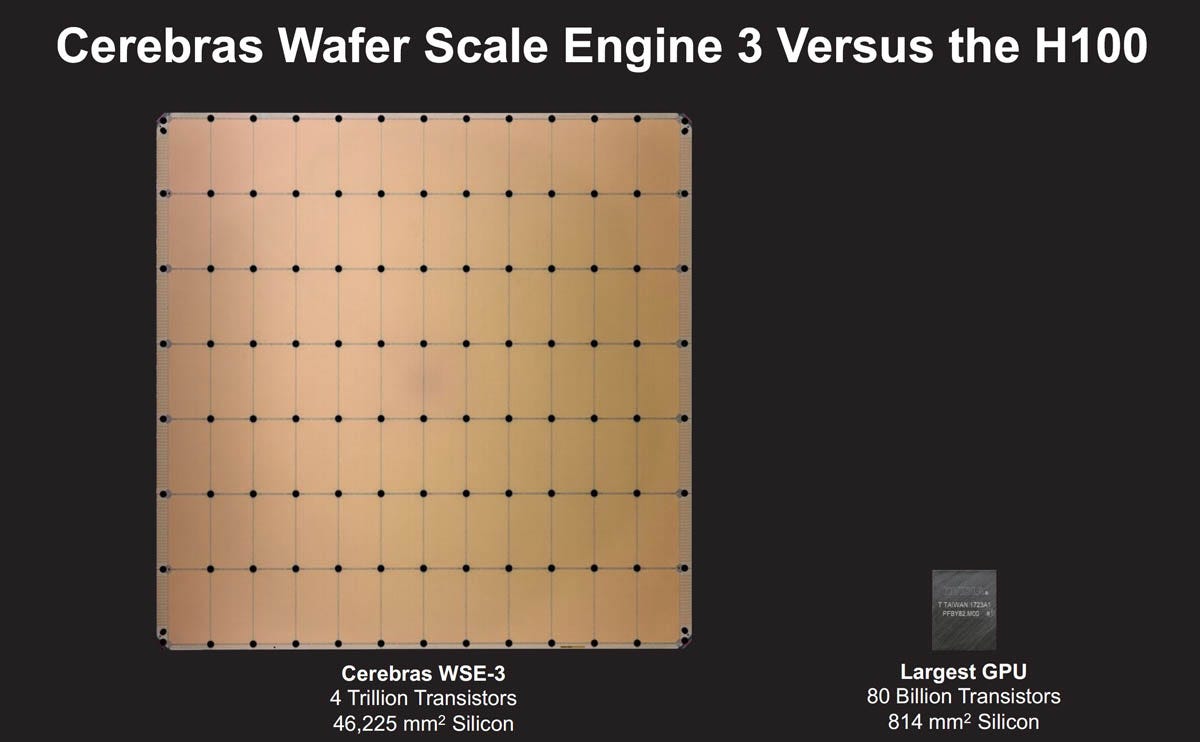
the WSE-3 is 46,225 mm², or ~57 times an H100. it has 44 GB of SRAM across 900,000 tiny cores, each with 48 KB wired to its compute unit. the aggregate bandwidth is 21 PB/s.
WSE-3 ridge point = 12.5 PFLOPS / 21 PB/s = 0.6 FLOP/byte
decode at batch 1 is about 1 FLOP/byte. on the WSE-3, that’s above the ridge point. the chip is compute-bound at batch 1! this doesn’t happen on any good old GPU.
so now that we have this background, the rest of this article will be about what it takes to actually build a chip like this, how they program it, and what are some of the hardest obstacles Cerebras faces in the road to be the ultimate NVIDIA killer.
Gene Amdahl tried wafer-scale integration in 1980 with Trilogy Systems. they raised $230 million raised, which was notably the largest startup round in Silicon Valley at the time. a prototype shorted out and heated “to a merry red glow” in front of executives. the wiring delaminated, the fab flooded, and the company president died. Amdahl was in a car accident, and the project was completely dead 5 years later. true story by the way.
Texas Instruments, ITT, and the NSA also all tried and failed.
the all arrived at a similar conclusion: to make this work, you need 99.99% yield, which very smart people at the time thought couldn’t happen for 100 years.
Cerebras was founded in 2015 by five people who’d all worked together at SeaMicro (sold to AMD for $334M). they’ve shipped three generations of a true wafer scale chip: WSE-1 (16nm, 2019), WSE-2 (7nm, 2021), WSE-3 (5nm, 2024).
they had to solve five problems that nobody had been able to solve before.
a 46,225 mm² chip at TSMC 5nm defect density (~0.001 per mm²) will have about 46 defects. on a normal chip, any one of those kills the whole thing.
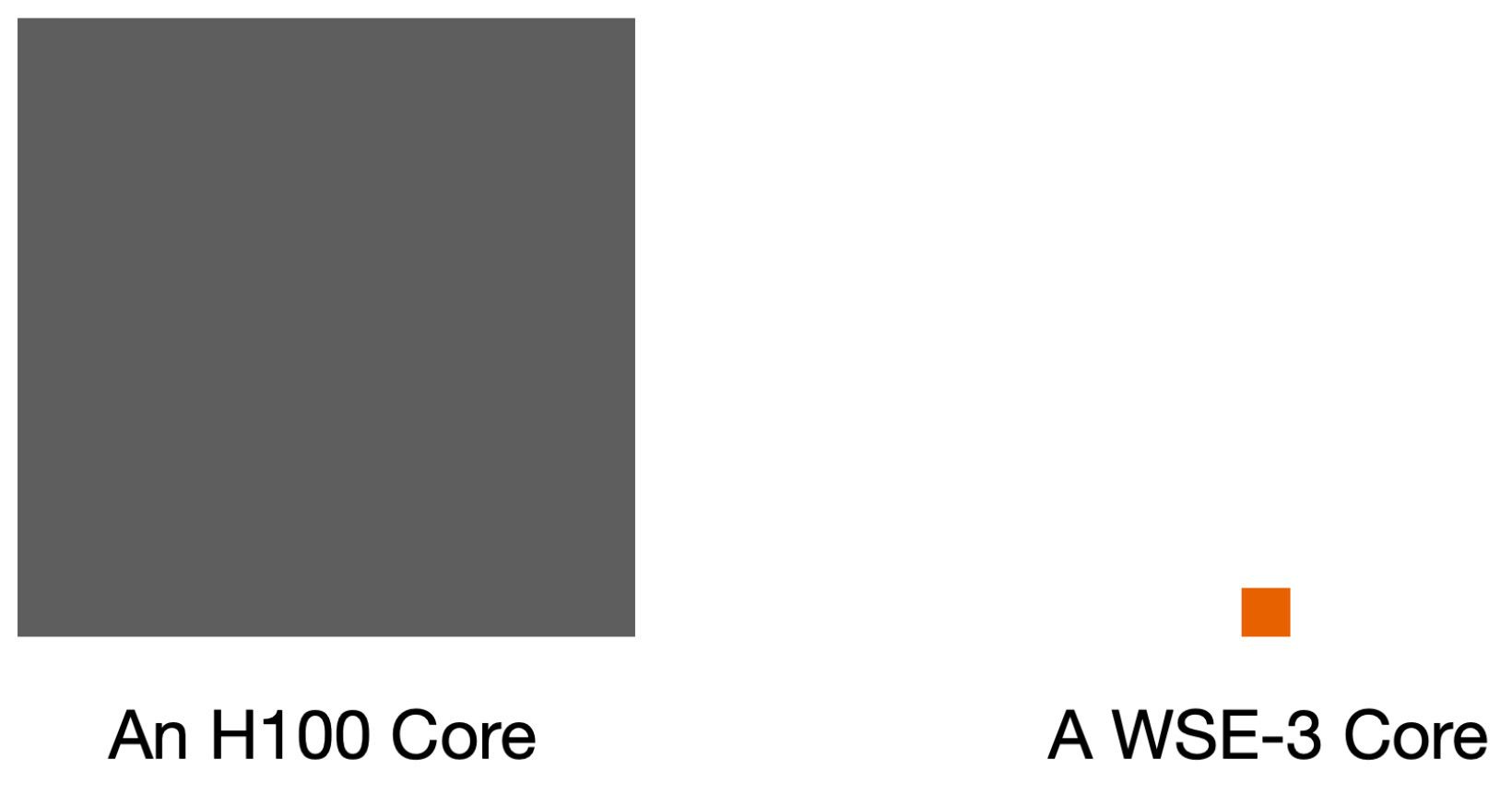
Cerebras made 970,000 tiny cores, each 0.05 mm², about 1/120th the size of an H100 SM (about 6 mm²). a defect kills one core, but importantly, it doesn’t kill the chip.
the WSE-3 ships with 900,000 active cores out of 970,000 physical, which comes out to about 93% utilization. the fabric just routes around dead ones. so from the software’s POV, the mesh is perfect.
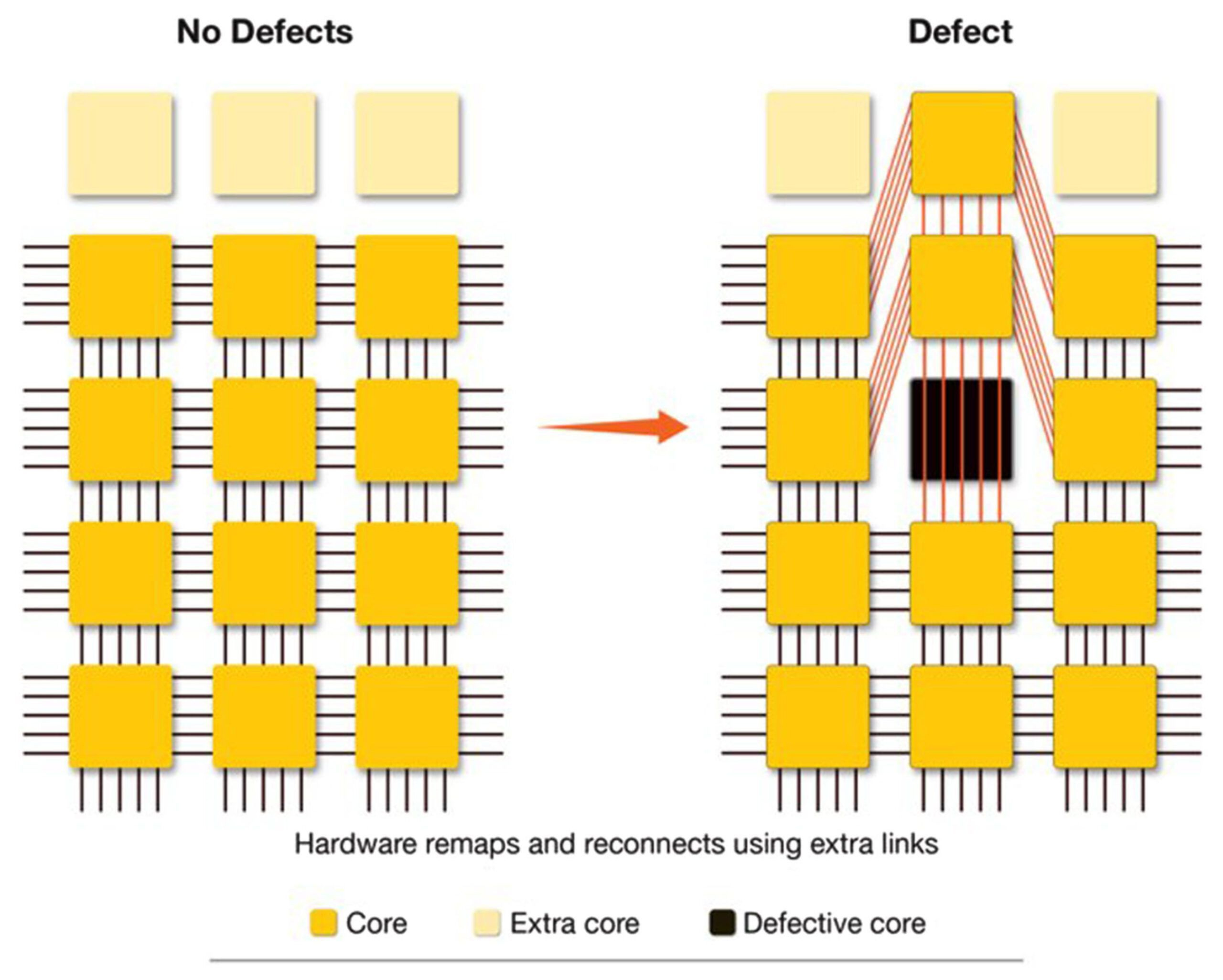
the yield problem was solved not by reducing defects but by making each defect cheap (economically viable to have these defects).
silicon expands at 2.6 ppm/K. FR-4 PCB: about 15 ppm/K. when the chip heats up, the PCB grows faster than the silicon. for a normal GPU (28mm on a side), the displacement at the corner during a 65°C swing is about 16 micrometers.
for a 215mm wafer: 122 micrometers at the corners. that’s the diameter of a human hair. 5-7x beyond the failure threshold of BGA, flip-chip, wire bonding, everything standard. but with this problem, every normal way to attach a chip to a board breaks.
Cerebras made a custom connector material that absorbs this displacement. the assembly is a four-layer sandwich: cold plate, wafer, custom connector, PCB. they had to build 100% custom machinery to assemble it.
23 kW from one wafer. more than 20,000 amps. if you deliver that through PCB traces from the edges, the voltage drop across 215mm works out to about 9.6V. the chip runs at about 1V.
they use vertical power delivery: 300+ VRMs distributed across the wafer surface, feeding current perpendicular to the silicon. each of the 84 die regions gets its own regulation.
i repeat: 23 kW from one wafer. air cooling was modeled and rejected, because the vapor chamber dries out. water cooling, custom copper cold plate with micro-fin channels, 100 liters per minute at 20°C.
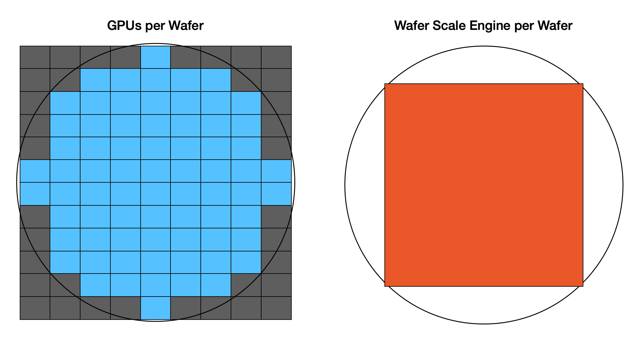
the WSE-3 is not one die. a lithography scanner can only expose 26mm x 33mm at a time (the “reticle”), so no chip can be larger than about 858 mm² from a single exposure.
what Cerebras does: TSMC prints 84 identical copies of the same die on the wafer, just like they’d print 84 normal chips. but instead of sawing the wafer apart, Cerebras adds extra lithography steps to pattern short wires across the scribe lines (the lanes between dies that normally get sawed through). the wires are less than 1mm, using upper metal layers. over 1 million wires cross die boundaries, and the protocol includes redundancy for defective wires.
from software’s perspective, the 84 dies don’t exist.
the mesh looks like one single chip (reminder: from the software POV).
this is the part that gets the least attention and i think it’s by far the most interesting. but i’m also biased because i <3 software and i’m a software guy.
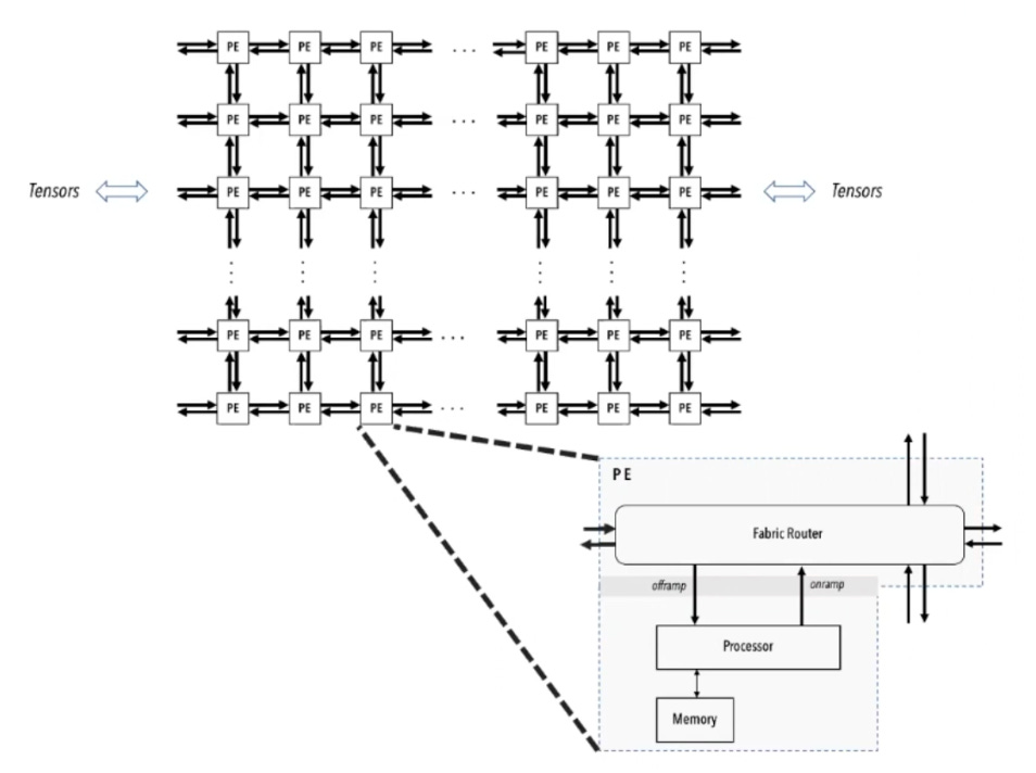
each core has its own program counter, its own 48 KB of SRAM (code AND data), and its own 5-port router (north, south, east, west, local). cores send 32-bit messages called wavelets through the mesh. each wavelet has a 5-bit “color” tag that determines its route and what task it triggers when it arrives.
this is a dataflow architecture. on a GPU, the program counter drives execution (warps run instructions in order). on the WSE, data arrival triggers computation. a wavelet arrives on a color, the bound task fires. no wavelet, nothing happens. if a weight is zero, no wavelet is sent. this is how they get unstructured sparsity acceleration, which GPUs can’t do because of how warps work (all 32 threads in a warp execute the same instruction).
the publicly available compiler has two modes.
layer-pipelined: the entire model maps onto the wafer at once. each layer gets a rectangular region of cores. data physically flows across the wafer from one region to the next. the compiler has to solve a VLSI floor-planning problem: assign non-overlapping rectangles, balance compute across layers, configure routing with 24 available colors. Cerebras published this as an NP-hard problem at ISPD 2020. this mode works when the model fits in 44 GB of on-chip SRAM. this is increasingly NOT true for the most used GenAI models out there today (April 1st, 2026).
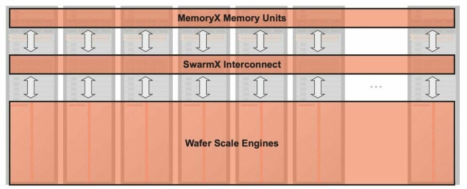
weight streaming (the current public default): one layer gets the entire wafer. weights live off-chip in MemoryX (DRAM + flash, up to 1.2 PB) and stream in layer by layer. all 900,000 cores process that one layer, activations stay on-chip, weights are discarded, next layer streams in. this collapses the hard floorplanning problem into a much simpler data distribution. scaling to 2,048 systems is pure data parallelism — change one flag.
this is the biggest software advantage over GPU clusters. running a 70B model across many GPUs requires tensor parallelism, pipeline parallelism, FSDP, and some combination of NCCL, DeepSpeed, and Megatron-LM. on cerebras you just define a variable --num_csx=n.
the compilation pipeline: PyTorch → XLA lazy tensor capture → CIRH (high-level IR) → CLAIR (linear algebra IR) → kernel matching against hand-optimized library → placement → routing → per-core executable. the graph must be static — no dynamic shapes, no data-dependent branching.
this is a hard requirement because the compiler solves placement and routing at compile time. you can’t reconfigure 900,000 PE routing tables at runtime!
for inference API users, none of this matters of course. the API is OpenAI-compatible. for HPC developers using the CSL SDK, you’re programming individual cores in a Zig-based DSL, configuring routing tables by hand, fitting code and data in 48 KB. it’s completely alien compared to CUDA: no threads, no shared memory, no kernel launches. the advantage is no synchronization and no race conditions. the disadvantage is that you’re basically doing chip routing in application code.
I/O gap. on-chip bandwidth is 21 PB/s. off-chip I/O is about 150-200 GB/s, which is a 133,000x gap. for models that fit in 44 GB, this doesn’t matter, everything is on-chip. but most important models don’t fit in 44GBs. the AWS deal, where Trainium handles prefill and Cerebras handles decode, is an admission that the chip isn’t great at prefill. prefill is compute-bound, which means Cerebras’s bandwidth advantage is wasted during prefill.
throughput crossover. the headline tok/s numbers are per-user speed. GPUs batch users together, so the same weight read serves everyone. at batch 10-20 on a single H100, aggregate throughput probably matches a CS-3. at batch 128+, a DGX H100 system produces thousands of aggregate tok/s at a fraction of the system cost. cerebras has never published aggregate throughput at high concurrency. this is the most important missing data point in their public materials.
SRAM scaling has stalled? the high-density SRAM bitcell has been stuck at 0.021 µm² from 5nm through 3nm and into 2nm. meanwhile HBM is scaling to 1+ TB by 2028. the capacity gap is widening.
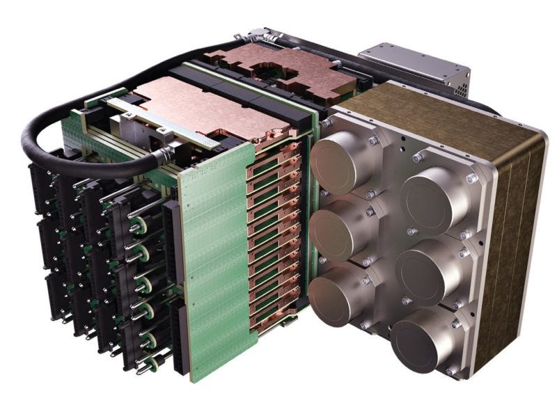
Cerebras solved (1) the yield math, (2) the compliant connector, (3) the vertical power delivery, (4) the cross-die interconnect. the Wafer Scale Engine is an important step in the history of computing. whatever happens to the business, it’s beautiful that a group of humans was able to make this technology work. WSE-2 is now part of the Computer History Museum, a beautiful museum in Mountain View you should definitely visit if you have the chance. It’s there with generational inventions such as ENIAC (the first computer) and the iPhone.
Subscribe to receive Peak FLOPS posts in your email! all posts are free.