
Budget silicon manufacturing.
Quarter Slots Are Here!
Get 1,000 custom silicon dies from just $2 per die
New quarter slot (0.5×0.5) option — 1,000 dies for $2,000 with Early Bird pricing.
Early Bird Deadline
Lock in early bird pricing for GF180MCU Run 3
Early bird pricing has ended — normal pricing now applies
Purchase Deadline
Final deadline to purchase a slot and submit your GDS
Too late, catch the next shuttle!
Submission Deadline
Final deadline to submit a clean GDS
See you in the next shuttle!
Complete Timeline
| Milestone | Date | Description |
|---|---|---|
| Campaign Opens | 1 August 2026 | Run 3 slots available for purchase on Crowd Supply |
| Early Bird Deadline | 30 September 2026 @ 11:59 PM AoE | Last day to purchase at early bird pricing |
| Purchase Deadline | 9 December 2026 @ 11:59 PM AoE | Final deadline to purchase slots |
| Submission Deadline | 16 December 2026 @ 11:59 PM AoE | Final deadline to submit clean GDS |
| Parts Shipped | Q2 2027 | Bare dies and packaged parts shipped to customers |
Ready to design your chip?
Your design. Your silicon. From $2 per die.
Get Started
- Project template — start your design from a working example
- PDK documentation — GF180MCU process design kit reference
- Slot specifications — die dimensions, pad rings, and I/O details
- Community Discord — chat with other designers and get free help
Need Help?
Professional design services are available from independent consultants experienced with the GF180MCU process. Whether you need a full custom design, help with verification, or guidance on your first tapeout, experts are ready to assist.
- Browse professional services — find a consultant for your project
- Join the Discord — free community support and peer help
Pricing
Slot Comparison
Choose the size that fits your design
| Feature | 1×1 Slot | 0.5×1 Slot | 1×0.5 Slot |
New! 0.5×0.5 Slot |
|---|---|---|---|---|
| Die Size | 3.93 × 5.12 mm | 1.94 × 5.12 mm | 3.93 × 2.53 mm | 1.94 × 2.53 mm |
| Die Area* | 20.12 mm² | 9.93 mm² | 9.94 mm² | 4.9 mm² |
| Core Area† | 12.92 mm² | 4.46 mm² | 5.02 mm² | 1.73 mm² |
| Default I/O Pads‡ | 56 | 56 | 56 | 48 |
| Max I/O Pads§ | 168 | 122 | 108 | 48 |
| Early Bird Price | $7,000 | $4,000 | $4,000 | $2,000 |
| Standard Price | $8,000 | $5,000 | $5,000 | $3,000 |
| Per Die (Early Bird) | $7.00 | $4.00 | $4.00 | $2.00 |
*Usable die area is smaller due to the seal ring (~26µm each side). Available with a custom pad ring or no pad ring.
†Core area = area inside the default pad ring.
‡Default pad ring I/O count. The default pad ring is only required if you purchase the Chip on Board packaging add-on.
§Maximum I/O with a custom pad ring from the LibreLane pad ring generator. You are free to use any pad ring configuration — or no pad ring at all.
$2.00 / die
USD $2,000
Early Bird
$3.00 / die
USD $3,000
Standard
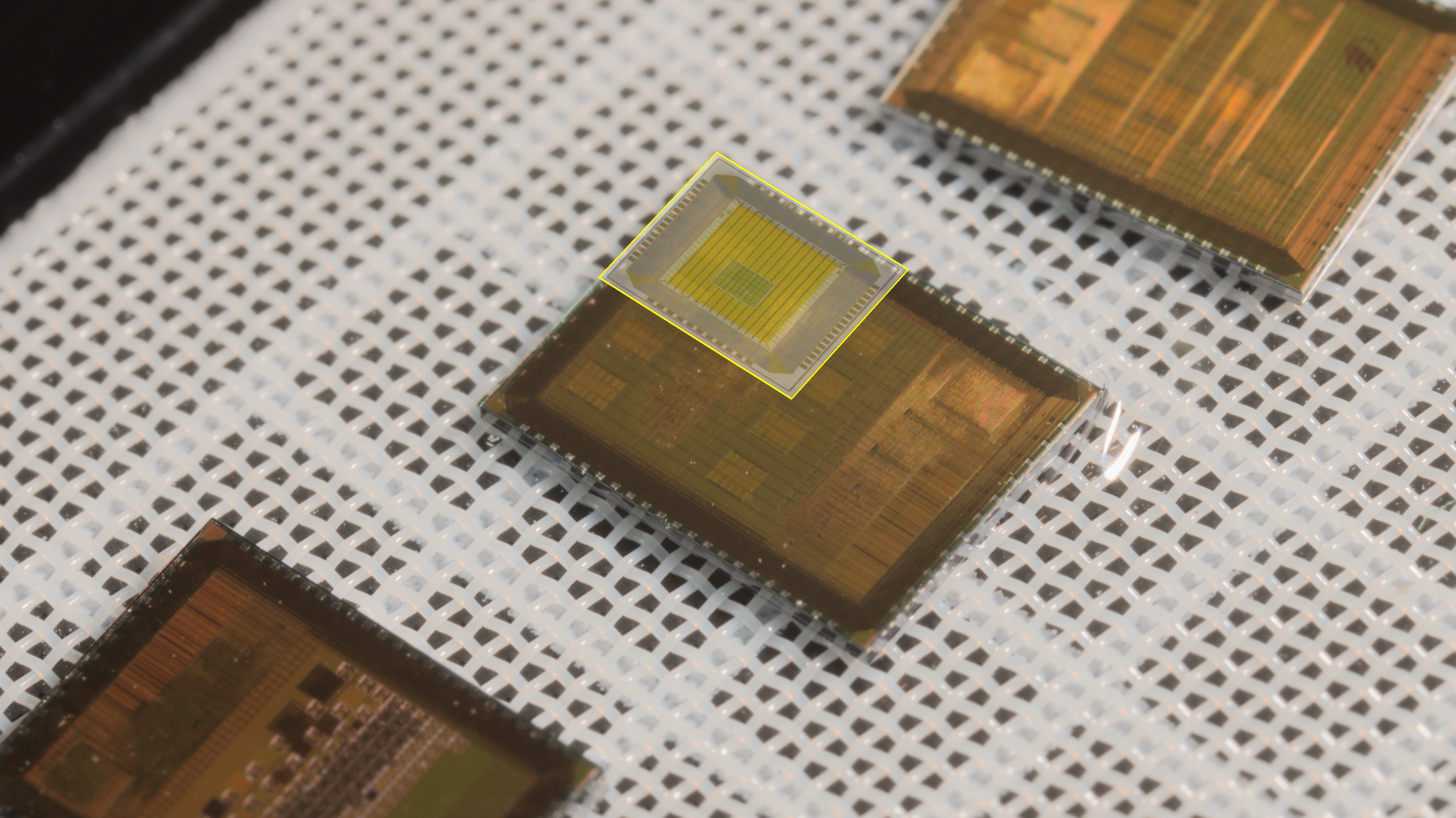
0.5×0.5 Slot (Quarter) New!
0.5×0.5 Slot — 1000 dies per slot
The quarter-size (0.5×0.5) slot is the smallest out of the bunch, but offers an unbeatable price point for prototyping designs without paying for silicon you do not need.
- GF180MCU process — 180nm mixed-signal
- Die size: 1.94mm × 2.53mm (4.9 mm²)
- Usable silicon: 4.67 mm² (custom pad ring or none)
- Core area: 1.73 mm² (default pad ring, required for COB)
- Default: 48 I/O pads — max: up to 48 I/O with custom pad ring
- 5 metal layers, MIM capacitors, poly & high-res resistors
$4.00 / die
USD $4,000
Early Bird
$5.00 / die
USD $5,000
Standard
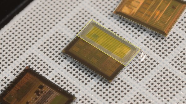
0.5×1 Slot (Half Width)
0.5×1 Slot — 1000 dies per slot
The half-width (0.5×1) slot delivers a tall, narrow die — ideal for I/O-heavy designs where signals concentrate along the long edges. Perfect for medium-complexity digital or mixed-signal projects, at just over half the cost of a full slot.
- GF180MCU process — 180nm mixed-signal
- Die size: 1.94mm × 5.12mm (9.93 mm²)
- Usable silicon: 9.57 mm² (custom pad ring or none)
- Core area: 4.46 mm² (default pad ring, required for COB)
- Default: 56 I/O pads — max: up to 122 I/O with custom pad ring
- 5 metal layers, MIM capacitors, poly & high-res resistors
$4.00 / die
USD $4,000
Early Bird
$5.00 / die
USD $5,000
Standard
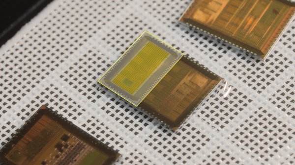
1×0.5 Slot (Half Height)
1×0.5 Slot — 1000 dies per slot
The half-height (1×0.5) slot gives you a wide, short die — ideal for designs that benefit from a wider core. Offers slightly more core area than the half-width slot at the same price.
- GF180MCU process — 180nm mixed-signal
- Die size: 3.93mm × 2.53mm (9.94 mm²)
- Usable silicon: 9.61 mm² (custom pad ring or none)
- Core area: 5.02 mm² (default pad ring, required for COB)
- Default: 56 I/O pads — max: up to 108 I/O with custom pad ring
- 5 metal layers, MIM capacitors, poly & high-res resistors
$7.00 / die
USD $7,000
Early Bird
$8.00 / die
USD $8,000
Standard
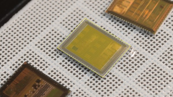
1×1 Slot (Full)
1×1 Slot — 1000 dies per slot
The full-size slot gives you the largest die area and maximum I/O count. Ideal for complex SoCs, full mixed-signal designs, or projects that need the most routing and core area.
- GF180MCU process — 180nm mixed-signal
- Die size: 3.93mm × 5.12mm (20.12 mm²)
- Usable silicon: 19.65 mm² (custom pad ring or none)
- Core area: 12.92 mm² (default pad ring, required for COB)
- Default: 56 I/O pads — max: up to 168 I/O with custom pad ring
- 5 metal layers, MIM capacitors, poly & high-res resistors
Enhance Your Order
Get your chips packaged and ready to test, or take home an entire wafer
Learn More
Add-on
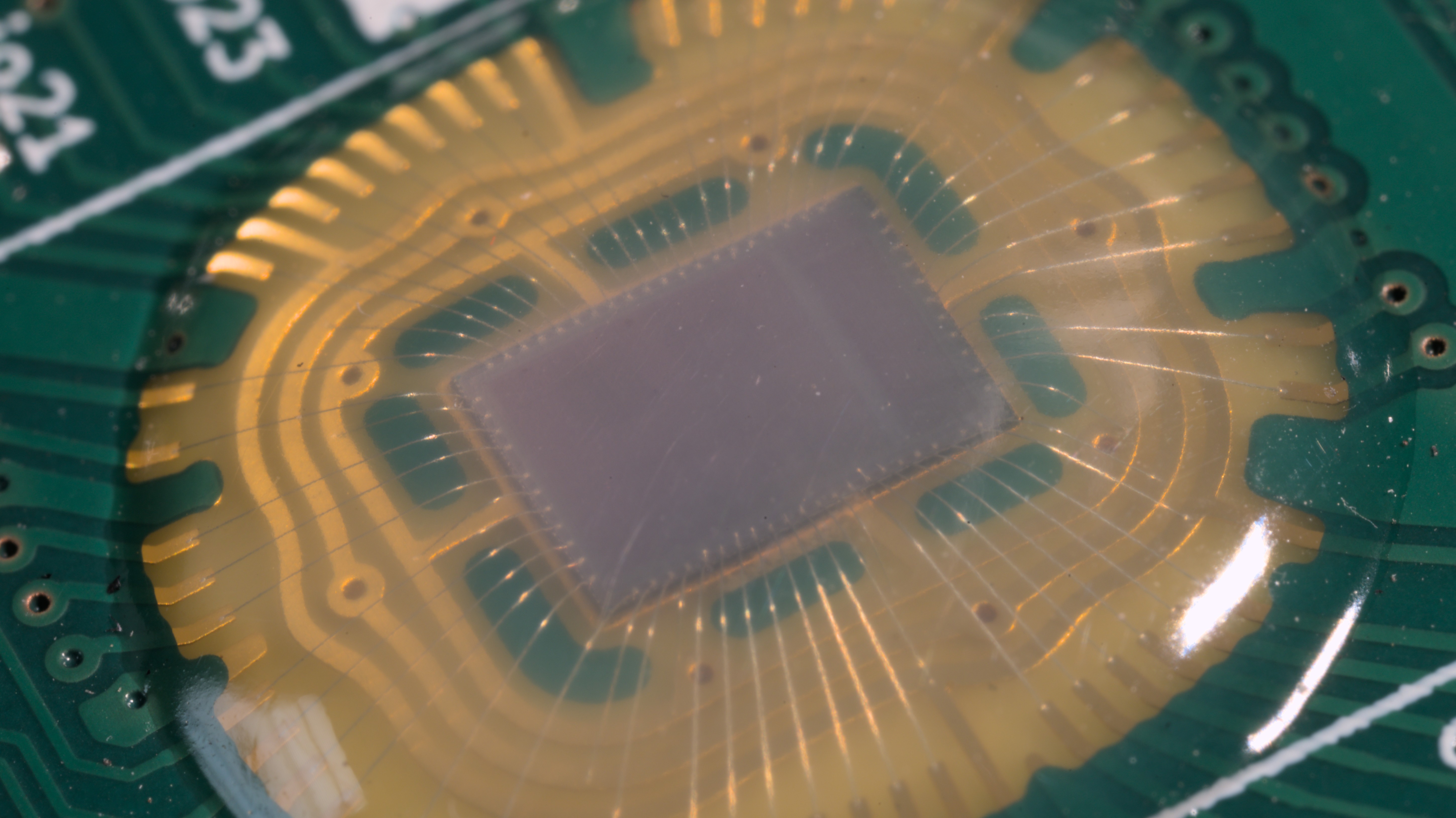
Chip on Board Packaging
$1,500 USD · $1.50 per die
Receive your dies wire-bonded onto small PCBs, ready for testing and integration.
- Wire-bonded onto individual PCBs
- Ready to power up and test immediately
- Requires the default pad ring for wire bonding
Add-on to any slot purchase. Requires the default pad ring.
Learn More
Add-on
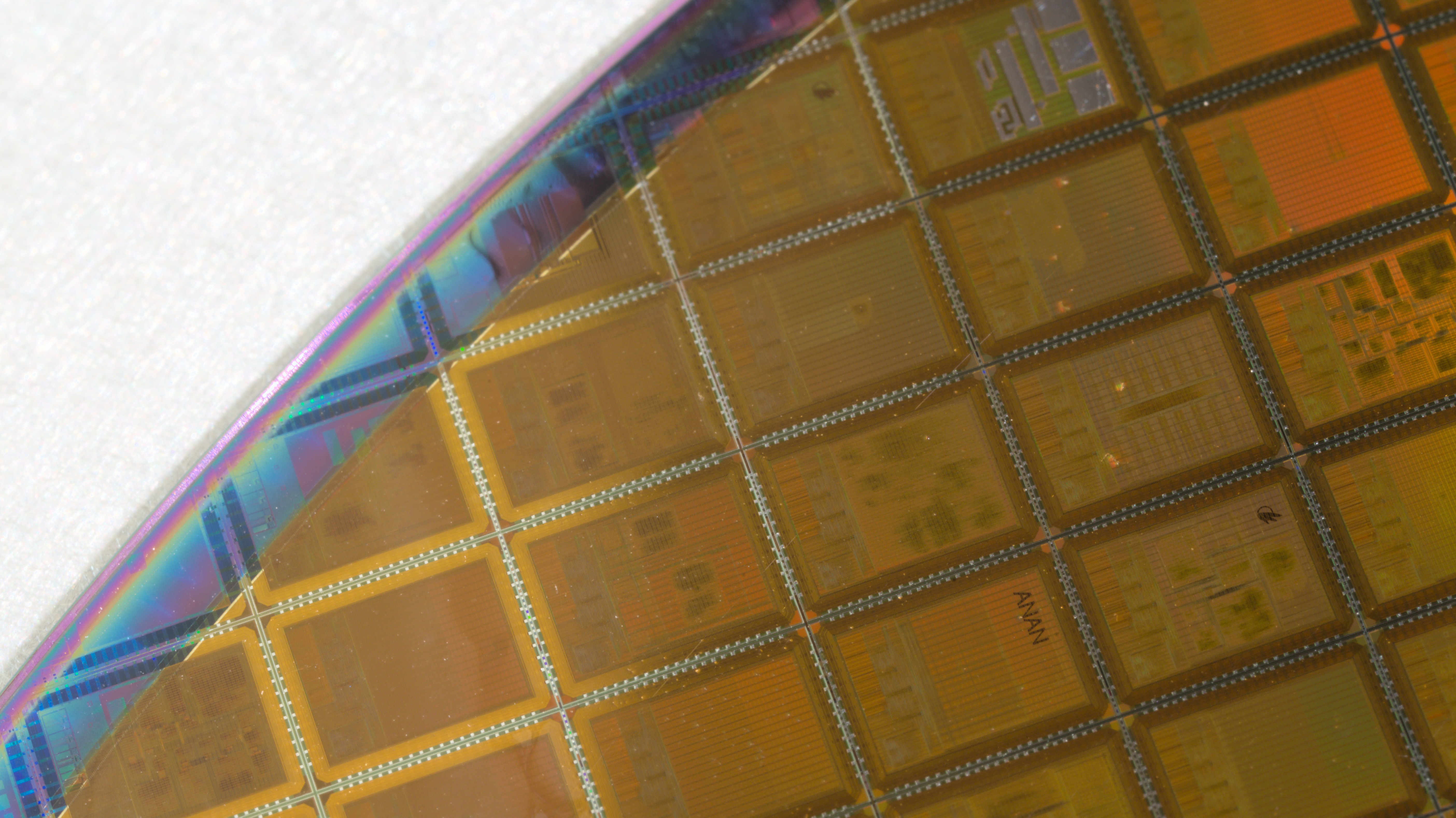
Full Undiced Wafer
$2,000 USD
Take home a complete 200mm wafer with your design alongside other Run 2 projects.
- Complete 200mm wafer, uncut
- Includes all designs from this run
- Perfect for custom dicing or display
Requires slot purchase
Technology
Technical Specifications
GF180MCU Process Technology Details
Slot Options
4 Sizes
1×1, 0.5×0.5, 0.5×1 half-width, 1×0.5 half-height
Metal Layers
5 Layers
Full routing capability
Quantity
1,000 dies
Per manufacturing slot
Capacitors
MIM & MOS
Metal-insulator-metal and MOS capacitors available
Resistors
Poly & High-Res
Multiple resistor types
Run 1: Many Designs on a Single Reticle
29 open-source designs from universities, startups, and hobbyists worldwide
Silicon fabricated and delivered
KIAN
1×1 slot
MOLE
1×1 slot
RBOY
1×1 slot
RZ80
1×1 slot
GD03
1×1 slot
TTP2
1×1 slot
2975
1×1 slot
ISHI
1×1 slot
WSLG
1×1 slot
What fits on 1 mm² of GF180MCU silicon?
Theoretical maximum standard cell density
Hard upper bounds — if you packed cells edge-to-edge with zero routing overhead
~14,320
Flip-Flop (FF_1)
per mm² theoretical max
~30,430
Buffer (BUF_4)
per mm² theoretical max
~39,380
3-input AND (AND3_2)
per mm² theoretical max
What Run 1 designers actually achieved
Real density from 24 designs on the GF180MCU shuttle
3k–14k
Typical Range
logic cells/mm² for most digital designs
across 24 designs
Achieved Logic Density by Design
Data from the Run 1 Density Report. Logic cell counts exclude infrastructure cells (fillers, taps, antenna diodes). “% of max” compares against buf theoretical max for each library (50k for 7-track, 40k for 9-track).
What fits in each slot?
Logic and memory capacity by slot type
Theoretical Logic Capacity (with default pad ring)
| Cell Type | 1×1 Slot | 0.5×1 Slot | 1×0.5 Slot |
New! 0.5×0.5 Slot |
|---|---|---|---|---|
| Flip-Flop (FF_1) | ~185,014 | ~63,867 | ~71,886 | ~24,774 |
| Buffer (BUF_4) | ~393,156 | ~135,718 | ~152,759 | ~52,644 |
| 3-input AND (AND3_2) | ~508,790 | ~175,635 | ~197,688 | ~68,127 |
Theoretical maximums with zero routing overhead. Run 1 designs typically achieved 10–44% of these values.
SRAM Capacity
| SRAM Type | Voltage | 1×1 Slot | 0.5×1 Slot | 1×0.5 Slot | 0.5×0.5 Slot |
|---|---|---|---|---|---|
| GF 5V sram512x8 | 5V | 40 kilobytes (80 blocks) | 20 kilobytes (40 blocks) | 20 kilobytes (40 blocks) | 10 kilobytes (20 blocks) |
| GF 5V sram256x8 | 5V | 28 kilobytes (112 blocks) | 14 kilobytes (56 blocks) | 14 kilobytes (56 blocks) | 7 kilobytes (28 blocks) |
| 3.3V sram1024x8 | 3.3V | 108 kilobytes (108 blocks) | 54 kilobytes (54 blocks) | 48 kilobytes (48 blocks) | 24 kilobytes (24 blocks) |
| 3.3V sram512x8 | 3.3V | 90 kilobytes (180 blocks) | 45 kilobytes (90 blocks) | 42 kilobytes (84 blocks) | 21 kilobytes (42 blocks) |
| 3.3V sram256x8 | 3.3V | 66 kilobytes (264 blocks) | 33 kilobytes (132 blocks) | 33 kilobytes (132 blocks) | 16.5 kilobytes (66 blocks) |
Block counts use die area minus seal ring (26µm each side). Run 1’s most SRAM-heavy design (RISCBoy-180) used 60 blocks in a full slot.
Get notified!
We'll email you when details are confirmed.