Nobel Prize winning economist, Paul Krugman, discusses TPUs and GPUs with Paul Kedrosky. No criticism of Krugman intended, it’s great that computer architecture is getting so much attention.
All of a sudden, everyone is talking - and writing - about Google’s TPUs (Tensor Processing Units). The use of TPUs to train Google latest, market leading Gemini 3 model together with Google’s decision to sell TPUs to third parties (apparently including arch-rival Meta) have combined to create a major ‘vibe-shift’ away from Nvidia and towards Google’s hardware.
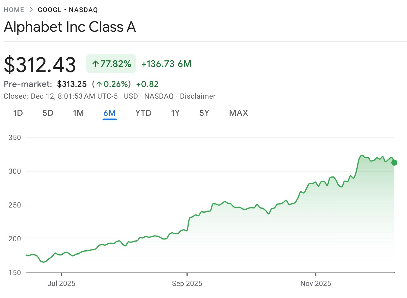
Not just a vibe-shift either as Alphabet’s stock price has been on a tear:
The coverage of the latest TPUs (v7) has been so extensive that, rather than add another series of takes, I thought it would more useful for readers to curate a selection of some of the most informative posts and links on TPUv7.
Before that, though, I wanted to briefly highlight several points that I can’t recall seeing much discussed elsewhere.
We looked at the origins of Google’s TPU programme in:
The origins of the TPU program date Google date all the way back to 2013 - almost a decade before the launch of ChatGPT - when it first became apparent that Google might need to start applying deep learning at scale.
The essence of the design dates back even further - into the 1970s. In their 1978 paper Systolic Arrays (for VLSI) H.T Kung and Charles E. Leiserson of Carnegie Mellon University had set out proposals for what they called a ‘systolic system’.
A systolic system is a network of processors which rhythmically compute and pass data through the system….In a systolic computer system, the function of a processor is analogous to that of the heart. Every processor regularly pumps data in and out, each time performing some short computation so that a regular flow of data is kept up in the network.
The approach didn’t gain widespread adoption in the 1970s and 1980s, but by 2013 the time was right:
By 2013 some of the original motivation behind Kung and Lieberson’s ideas had fallen away, particularly dealing with the limits of fabrication technology of the 1970s, had fallen away. However, the inherent efficiency, and of particular relevance in 2013, the relatively low power consumption, of this approach for tasks such as matrix multiplication remained. So the TPU would use systolic arrays.
We discussed the first Google TPU’s architecture in more detail in:
With the benefit of hindsight this first Google design seems remarkably primitive. It was a co-processor attached to a CPU via a PCIe interface, could only perform integer arithmetic, and was only useful for inference. But it met the design objectives of being cost effective, deployable at scale and was in Google’s datacenters by 2015, just 15 months after the start of the project.
The reveal of TPUv1 led to - as the TPU team would later quip - “the launch of a thousand chips”:
Intel went on a buying spree of companies with a domain specific architecture (DSA) for ML: Nervana, Movidius, MobilEye, and Habana. Hyperscalers like Alibaba and Amazon and end users like Tesla started their own inference DSA chips. The venture community also reacted, investing $3B per year from 2016 to 2020 in more than 100 ML DSA startups. Some startups bet on novel ideas that didn’t succeed for general purpose computing such as analog computation, asynchronous logic, and wafer scale hardware. (It’s unclear today if the startups made the same investment in their software stacks for ML as they did in their hardware.) Inside Google, we’ve announced four successors to TPU v1 so far. Drawing an historical analogy to Helen of Troy—“the face that launched a thousand ships”—we say tongue-in-cheek that TPU v1 “launched a thousand chips.”
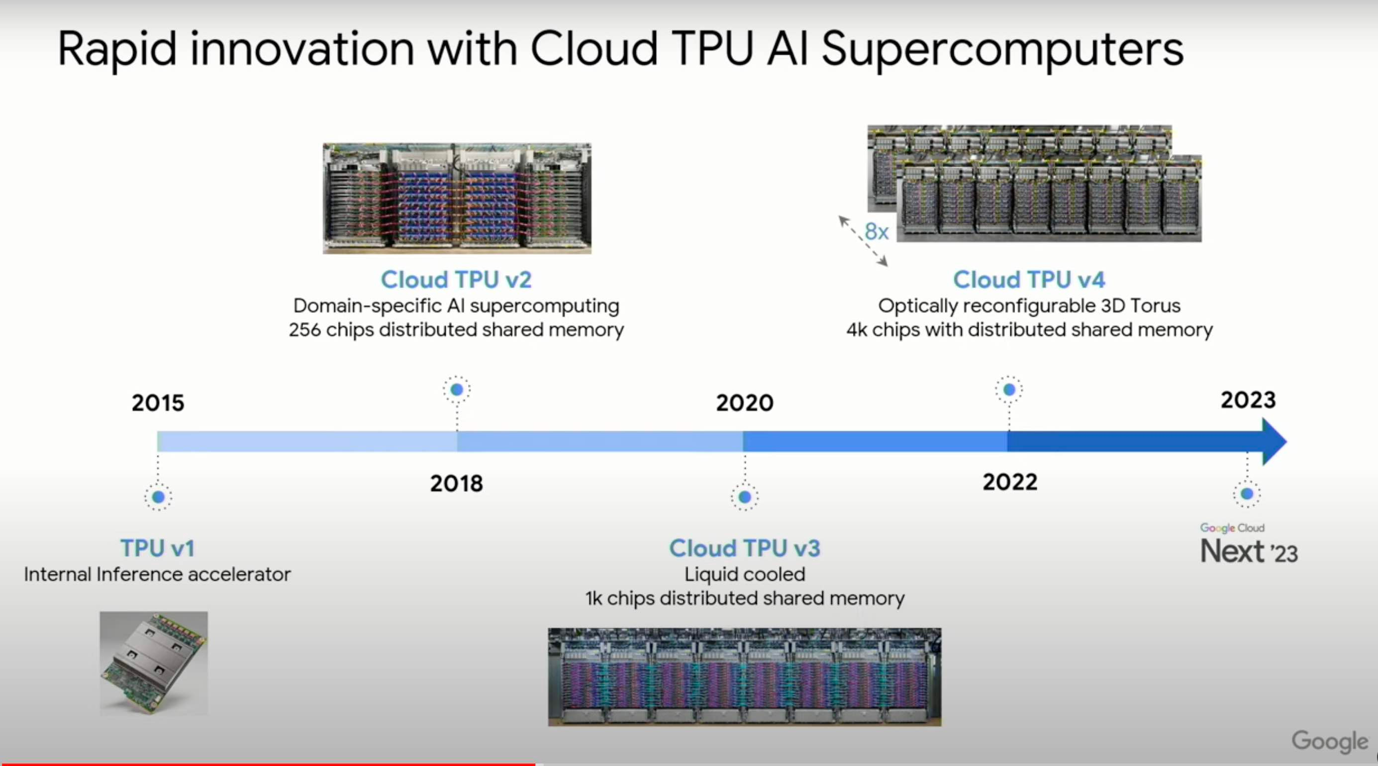
Some of those designs have fallen by the wayside but Google has stayed the course with incremental, but still significant, improvements in each successive generation:
TPU v2 (2017)
Inference and Training
High Bandwidth Memory (HBM)
Two Matrix Multiply Units per chip using floating point (bfloat16)
TPU v3 (2018)
As TPU v2 but with more memory bandwidth, higher clock frequency
Four Matrix Multiply Units per chip
TPU v4 & TPU v4i (2021)
Inference and Training (TPU v4) with liquid cooling or Inference (TPU v4i) with no liquid cooling
TPU v5p (performance) & TPUv5e (economy) (2023)
“Designed for performance, flexibility, and scale, TPU v5p can train large LLM models 2.8X faster than the previous-generation TPU v4. Moreover, with second-generation SparseCores, TPU v5p can train embedding-dense models 1.9X faster than TPU v42.”
TPU v6e (2024)
“Trillium TPUs achieve an impressive 4.7X increase in peak compute performance per chip compared to TPU v5e. We doubled the High Bandwidth Memory (HBM) capacity and bandwidth, and also doubled the Interchip Interconnect (ICI) bandwidth over TPU v5e. Additionally, Trillium is equipped with third-generation SparseCore, a specialized accelerator for processing ultra-large embeddings common in advanced ranking and recommendation workloads.”
TPU v7 (2025)
See the end of this post for links to much more reading on Google’s latest TPU.
We can perhaps compare Google’s journey with TPUs to Apple’s program to design it’s own System-on-Chips first for the iPhone, then the iPad and more recently the M-series for the Mac. Incremental improvements each year and ‘Apple Silicon’ has clearly become a key part of Apple’s strategy.
And of course Apple has major advantages with it’s control of the complete hardware and software stack, which takes us to …
I liked the opening of this detailed post on Google’s TPUs:
There is mythological reverence for Google’s Tensor Processing Unit. While the world presently watches NVIDIA’s gravity drag more companies into its orbit, there sits Google, imperial and singular.
I’m not sure that Google’s TPU program is singular, but it certainly stands out in the crowd of the ‘thousand chips’. Let’s list some of the advantages it has over competitors (including, in many cases, Nvidia):
A tiny number of competitors can match the financial resources that Google can apply to its TPU development program;
Full control over the stack - including software and machine learning algorithms - that it applies in its services. That control means that there can be feedback into the hardware design as software and algorithms evolve;
Decades of experience of building and operating data-centers at scale;
No legacy (non-AI applications) to support.
The fact that Google was first with an AI accelerator in 2015 shows how these advantages and feedback can operate in practice.
And the fact that this has happened within an organisation as large and with fingers in many pies doesn’t seem to have held development of the TPU series back. There has been more to the evolution of the TPU architecture than just the capabilities of individual TPU chips. By v4 the TPU project had moved from creating a peripheral that can be attached to one of Google’s existing servers (in v1) to ‘Cloud AI Supercomputers’ that can work independently and combine thousands of chips with shared memory and high-speed interconnect.
Next, the dilemma that Google must have faced in its decision to sell TPUs. After all Google has been making TPUs since 2013, so why wait until 2025 to sell them externally?
Part of the answer is probably that almost all potential customers are competitors of Google’s core businesses.
And competitors can benefit, even without buying any TPUs. SemiAnalysis, with tongue in cheek a little perhaps, commented that Google’s decision to sell TPUs had already saved OpenAI billions of dollars.
As Liberty has pointed out this discount is in the form of equity investment which is not quite the same as cash, but still.
This prompted some musing on Substack Notes on the dilemma that Google must have faced:
I’d love to have been a fly on the wall for Google’s decision to sell TPUs externally.
On one hand:
Add value by capturing the margin on TPU sales and gain economies of scale.
On. the other:
Help your biggest (and in extremis an existential competitor) OpenAI to grab a big discount on the chips that they need to compete with you.
Not an easy decision. What would you do?
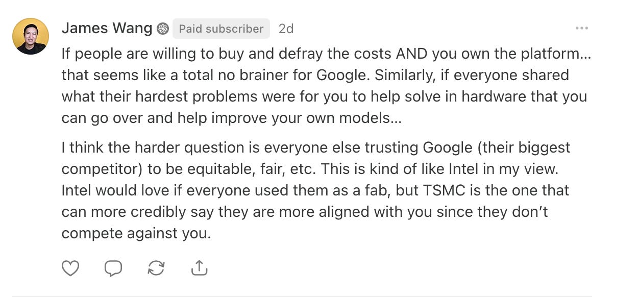
The reaction to this was pretty overwhelmingly on the side of ‘sell the chips’. James Wang’s typically thoughtful response was probably closest to my own thinking.
I suspect that the key factor is the degree of control that remains with Google. It can decide, on a year by year basis, who gets TPUs and how many TPUs they get.
If Google were to be truly evil (and they gave up on ‘don’t be evil’ many years ago) they would get their customers dependent on TPUs only to cause chaos by pulling out of the market. But, perish the thought, Google would never drop an important product, would they? See the Killed by Google for a few (or rather, very many) counter-examples.
A key takeaway from this is that none of these potential TPU customers should really make themselves reliant on Google, which by itself will limit the uptake of TPUs.
The final point is that there hasn’t been much discussion of the merits of TPUs as an architecture versus GPUs. I think this is largely because there are some implicit assumptions underpinning much of the commentary:
GPUs are better for training;
TPUs are more cost effective for inference, but you probably have a lot of older GPUs around that are perfectly good enough for inference.
Google’s exclusive use of TPUs to train Gemini 3 undermines the first part of this narrative somewhat.
It’s safe to say though that at this point we still don’t know who will ‘win’ in the GPU vs TPU competition. Or rather, as I don’t think that there will be a single winner, what the respective market shares of each design will be.
I don’t think that the merits of the respective architectures will determine the outcome; the quality of the respective contenders on each side will be much more important.
I do think we are likely to see a degree of convergence between the two approaches. Over the years Nvidia’s GPUs have reduced their support for higher precision floating point (FP64) calculations and added matrix multiply units (added in 2017 with the Volta architecture) making them more specialised for AI and architecturally closer to TPUs.
In any event the competition between the GPUs and TPUs (and not just between Nvidia and Google) looks likely to be the most interesting and keenly fought architectural contest since CISC vs RISC in the 1980s.
Now onto the some of the highlights of recent writing on the TPU, starting with Google’s announcement:
Onto the analysis: first SemiAnalysis (paywalled but with 9,500(!) words before the paywall) which covers, amongst other topics:
Revisit our original TPU deep dive with a refresher on the TPU hardware stack from silicon down to the software layer.
Cover the positive developments on the open software ecosystem front as well as the critical missing ingredient for Google to make the TPU ecosystem a viable challenger to the CUDA moat: open source their XLA:TPU compiler, runtime, and multi-pod “MegaScaler” code.
In the paywall, we will discuss the implications for Nvidia’s moat and compare Vera Rubin to the next gen TPUv8AX/8X (aka Sunfish/Zebrafish)
Also cover the long term threat to Nvidia.
The coverage of developments in the ‘open software ecosystem’ is particularly fascinating.
Today, I would like to introduce the Google Ironwood TPU rack and its Optical Circuit Switch (OCS) system, which have recently attracted much attention from investors.
And finally an interesting post from Phabian (free) on the TPUv7 supply chain:
Google Inc’s Ironwood (TPU v7) is one of the least transparent but most important AI accelerators in production. The full bill of materials is not public, but if you stitch together Google disclosures, OCP (Open Compute Project) standards work, and industry supply-chain research on CoWoS, HBM, optics, and OSATs, a reasonably clear map emerges of who actually gets paid when Google ships another Ironwood pod.
This article turns that long vendor list into a narrative: how the stack fits together, and where the highest operating leverage to Ironwood volume really sits.