Intel has bounced back from its, at one point, seemingly existential crisis. When I wrote this post back in August 2024 the situation seemed bleak.
Today Intel’s share price has risen to almost $100.
Central to Intel’s resurgence is surging demand for the product that has sustained Intel over almost five decades: the CPU or more specifically x86 CPUs.
So it seems like a good time then to go back to the design that represents the real start of Intel’s CPU story; a CPU architecture that Intel didn’t create and was almost shut down before it got started.
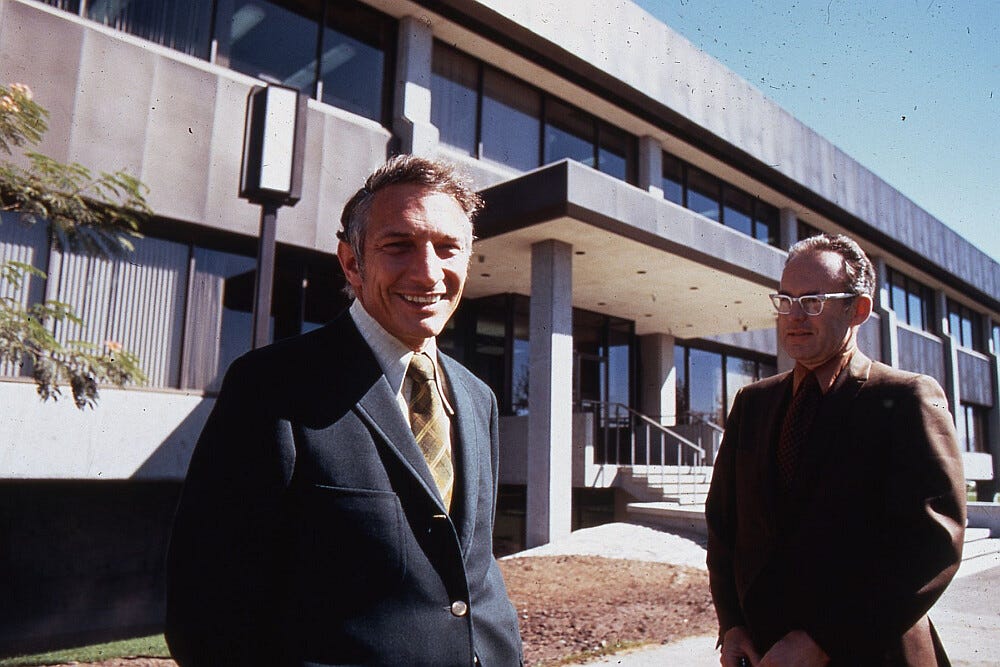
Robert Noyce was torn. The co-inventor of the integrated circuit, co-founder and CEO of Intel, the ‘Mayor’ of Silicon Valley, had patiently sat in his office listening to the proposal for three uninterrupted hours. Finally he stood up and put his hands on his desk. The answer was ‘no’:
‘It’s intriguing and we can do it. We can take a shot at it - but it’s a useless product, and making it would not be in our business interest.’
The proposal? An 8-bit microprocessor.
More precisely, the first 8-bit microprocessor.
Across the table from Noyce were Gus Roche and Jack Frassanito from Computer Terminal Corporation (CTC) of San Antonio Texas. CTC had already announced the innovative Datapoint 3300, one of the first computer terminals with a cathode-ray-tube-based display. Now, early in 1970, they were working on the 3300’s successor, the Datapoint 2200, a slimmed-down terminal in a box the size of an IBM Selectric typewriter.
At the heart of the 2200 would be a simple computer whose architecture had been designed over Thanksgiving weekend in 1969 by engineers Vic Poor and Harry Pyle. Squeezing that computer - constructed using the Transistor-Transistor Logic (TTL) and Medium Scale Integration (MSI) components then widely available - into the limited space available in the 2200’s casing would be a major challenge.
For more on the origins of CTC, the Datapoint 2200 and its architecture:
Personal Computer Origins: The Datapoint 2200

As We May Think, The Mother of All Demos, The Xerox Alto; all were breakthroughs in thinking about how to make the computer more personal. They were not, however, the true antecedents of the first ‘personal computers’. Instead, that line of descent runs through something much less visionary, capable or expensive: the humble computer terminal.
One possible solution was soon clear to the CTC team: create a custom design using the latest Large Scale Integration (LSI) technology to replace several TTL and MSI components.
Who could create such a design? CTC was already working with a start-up chip-maker, based in Santa Clara, California. That chipmaker was, of course, Intel. Perhaps they could help?
Noyce had founded Intel Corporation, with Gordon Moore, in June 1968. In its early years Intel’s strategy focused on memory chips: the first Intel product was the 3101 a 64-bit static random-access memory (SRAM) followed by the 3301 Schottky bipolar 1024-bit read-only memory (ROM) and the the 256-bit 1101, the first commercial metal–oxide–semiconductor field-effect transistor (MOSFET) silicon gate SRAM chip. Two dynamic random access memory (DRAM) chips, the 1102 and 1103 would follow in 1970.
There was a good reason for this focus on memory. Semiconductor memory was on track to eclipse and replace the use of core memory in mainframes and minicomputers. Intel, operating at the leading edge of chip manufacturing, had a clear opportunity to create a business with both substantial scale and attractive margins.
There was a third alternative to SRAM and DRAM for volatile memory storage. ‘Shift registers’ only allowed individual bits to be written and read one by one in a predetermined order. For some applications, such as storing the characters displayed on a CRT screen, where patterns of access to memory were predictable, they were a viable, and cheaper, alternative to SRAM. CTC’s Datapoint 3300 used shift registers manufactured by Texas Instruments: 54 of TI’s 200-bit TMS4100, enough to store the 1,800 6-bit characters displayed on the 3300’s screen. Soon Intel was developing a 256-bit shift register to try to capture some of that market too.
Part time Intel sales representative - the start-up could not afford to employ him full time - Art McDowell had made a trip to San Antonio late in 1968 to meet CTC co-founder Phil Ray. The meeting would soon become famous. McDowell would later recall:
‘At the end of the conversation I … showed him the data sheet for the [Intel] shift register. At the time, 256 was big. Phil suggested that I should be wearing a Santa suit and said ‘Damn can these guys ship this? Can they meet National’s [National Semiconductor’s] price? I got on the phone to Intel and they came unglued. We met the price. I wrote a million dollar sales contract that very day.’
Intel’s sales in 1969 would total $370,000. Those shift register chips, destined for CTC’s second product, the Datapoint 2200, wouldn’t ship until 1970 but with one stroke of the pen CTC had placed itself amongst Intel’s biggest customers.
Both Intel and CTC had to create their products though. It would be a year later at the end of 1969 before CTC had a specification of the Datapoint 2200’s architecture, created by recent recruit Victor Poor over a single Thanksgiving weekend. Just a few weeks after that architecture was created Poor found himself in a series of meetings in Intel’s offices, scheduled to discuss progress on Intel’s 256-bit shift registers design.
Poor was aware of the challenges of fitting his design into the 2200’s box. Whilst he was at Intel, why not see if they could create a custom chip to replace several of its TTL and MSI components?
In the first meetings the response was unremittingly negative. Intel was only interested in high volume parts, not custom low-volume designs. The hosts did mention that they were working on a 4 -bit CPU for a calculator - a design which would later be marketed as the Intel 4004 - was mentioned but Poor quickly recognised that this would be inadequate.
Finally, having just finished a meeting with future Intel CEO Andy Grove, Poor found himself alone with Intel engineer Stan Mazor and the conversation turned to one possible custom design for the 2200, an SRAM with some additional logic to support a push-down stack. Poor explained that this would form part of the CPU of a simple 8-bit computer he was working on.
Meeting Mazor was fateful. The Intel engineer had recently been working on the design of the 4-bit CPU for Japanese calculator maker Busicom. Sure, he told Poor, Intel could create the stack. It could even add an arithmetic and logic unit. In fact, having designed a 4-bit CPU for the calculator, it was ‘not a big leap to make an entire 8-bit CPU on a chip’ and Intel could do that too.
There was one, elephant sized, problem though. Mazor had helped create the specification for a 4-bit CPU, but that was as far as the project had progressed. As a hugely stretched start-up designing and making several innovative memory products, it didn’t have the resources - at the end of 1969 Intel had only around 100 employees - to make the 4-bit CPU, let alone a brand new 8-bit design.
Federico Faggin, who was about to join Intel and lead the creation of that 4-bit CPU, would comment on Mazor’s assertion that ‘This was indeed a bold statement to make given that Stan was not a chip designer’. Sometimes, however, fate favours the bold!
After the meeting Poor sent Mazor the programming manual for his architecture and following discussions and a few suggested simplifications - such as deleting instructions that he viewed as too complex - Mazor created a technical proposal for a single chip 8-bit CPU.
The two firms still needed to agree commercial terms, so CTC’s Roche and Frassanito soon made their way to Robert Noyce’s office in Santa Clara to negotiate.
The CTC proposition was simple: Intel could have the Datapoint 2200’s instruction set for free and could sell the chip implementing the architecture to any one. All CTC wanted was to be able to buy it. If CTC found the idea of an 8-bit single chip CPU compelling then surely others would too. Intel would be bearing most of the risk though, investing to develop the 8-bit CPU a product with an uncertain market.
So it wasn’t too surprising that, as we’ve seen, Noyce initially rejected the proposal. The rationale - Intel’s focus on higher volume memory chips - makes sense. Noyce had, in contrast to Andy Grove, backed the 4004 but a calculator chip had a much bigger, and proven, potential market. Perhaps Noyce was also wary of taking on too many custom projects. Perhaps too he was nervous about creating a more powerful CPU design that might compete with the same computer makers who he wanted to buy his memory chips.
Even so, Noyce must have been nervous about saying no to one of his biggest customers. Roche tried to make the deal more attractive by offering to fund development, which was enough to get Noyce to quickly reverse his decision. The meeting ended with the two sides agreeing to work together on the CPU.
The precise details of the final agreement made between Intel and CTC remain uncertain. The documents have been lost and all of the participants have a different recollection. Was it - as variously suggested - $50,000 up front, an agreement to buy 100,000 units for $30 each, or even a bet where Intel would receive $100,000 if it developed the chip in 6 months or pay CTC the same amount if it failed? We’ll probably never know. In any event Noyce, always looking for ways to generate cash for his rapidly growing start-up, got a deal that he believed was in Intel’s commercial interest.
An agreement was one thing, but turning that into a real chip required a whole lot more to happen and for a long time it looked very unlikely indeed. First of all Intel needed to recruit someone who would work on the project. Hal Feeney joined Intel from General Instrument in March 1970 and was immediately assigned to the development of the CTC CPU.
Just as significantly for the project, Federico Faggin joined a long list of Fairchild engineers who would be tempted away to join Intel, arriving three weeks after Feeney with the two men sharing an office (and even desk drawers) for a period.
In his first months at Intel, Faggin devoted all his energy to the development of the 4-bit calculator CPU. Feeney made some progress with the CTC CPU - now called the 1201 - but found himself being pulled into helping out on various memory products. The low priority given to the 1201 is unsurprising. Amongst Intel’s senior management, Noyce as we’ve seen had been equivocal about the project and Andy Grove, then grappling with low yields on Intel’s memory products, was actively and vehemently opposed to anything that he viewed as a distraction.
Meanwhile CTC had discovered that they didn’t actually need a single-chip CPU for the Datapoint 2200. Squeezing the TTL and MSI processor design into the 2200’s box was difficult but, in the end, proved to be possible. TTL chip prices had collapsed at the start of 1970, making the price agreed for the 8-bit processor unattractive. CTC shipped the TTL/MSI version of the 2200.
Progress on the 1201 ground to a halt.
Then, as 1970 drew to a close, another potential customer emerged. Japanese electronics manufacturer Seiko wanted to make a programmable desktop calculator to compete with Hewlett Packard’s offerings. Here, at last, was a volume application for the 1201.
At the start of 1971, after months of exhausting work days often stretching into the early hours of the morning, Faggin’s work on the 4004 and its companion chips was complete and he would turn his attention to the 1201. The design was soon renamed as the 8008 as an 8-bit successor to the 4004, a source of confusion ever since as the two architectures have nothing in common. Hal Feeney too was at last freed up from his memory duties and returned to the project working under Faggin’s supervision.
Then, in June 1971, came a bombshell. An new issue of Electronics magazine appeared with a full page advertisement from Intel’s arch-rival Texas Instruments which started proclaiming, perhaps somewhat provocatively, TI’s MOS capabilities:
MOS: the thrust is economy, complexity and volume.
TI has the capability-across the board.
MOS can put a computer on a chip.
MOS can cut system costs.
MOS can be economically customized and produced in big volume.
Or small.
Just anyone’s MOS? No. And that’s why you should carefully com-pure manufacturers’ capabilities.
Can they, for example, give you the full advantage of the complexity inherent in MOS-like putting 6,000 devices on a single chip? Can they optimize your system costs by building bigger, more complex chips-and still keep yields up and prices down?
What followed was the real shock, as below a picture of a what was clearly a CPU on a chip,
The device pictured here is a complete eight-bit parallel processor on a 215 by 225-mil chip. It includes an 8-bit parallel ALU with hardware, parity flags, an 8-bit accumulator with file registers, 8-bit program and memory address registers, and a multilevel program address stack. Tl developed and is producing it for Computer Terminal Corporation for use in an “intelligent” terminal, the Datapoint 2200 terminal. With its associated random access memory system, the 2200 has the capabilities of a full 8-bit mini-computer.
TI leads the industry in the ability to produce complex devices on large, cost-efficient chips.
Not just any CPU then, a CPU for the CTC’s Datapoint 2200. A TI version of the 8008!
Stan Mazor would capture Intel’s sense of disbelief.
“It was not hard to see that it was the 8008 done way ahead of us. We were just blown away—it was like finding that your partner is cheating on you. We were amazed and unhappy.
“Normally, when I give a customer a chip specification I have them sign a non-disclosure agreement, saying this is something we are working on and you are not to release it to a third party. I never did that with CTC, since the specification was custom with them. And I was young and naive and it never occurred to me to do that. But, unknown to me and Intel, my handwritten proposal went to TI, and they started a crash program. When we put down the program due to CTC’s financial problems, TI did the opposite and used automated tools to get the design done faster than we would have otherwise.”
TI Engineer Gary Boone would deny receiving any proprietary Intel information:
“... CTC and the principal architect there, whose name is Vic Poor, gave me a requirements document. Initially, I tried to do it on three chips using conventional design methodology. He told me that was unacceptable, saying “Intel can do it on one.” That is the first time I had heard about Intel on that project.
So we got sent home. CTC was in San Antonio, and TI was in Houston. So we got sent home to Houston to rethink whether we were going to give up or try to do it on one chip. We received what you might reasonably characterize as hints about Intel doing a better job than we were, or Intel promising a better result than we promised. In any event, we implemented an original design, TMX-1795 design, [and later, slightly revised design, called TMX-1795A], to meet Mr. Poor’s requirements, including his one-chip requirement. Any assertion that we improperly received information belonging to anybody else is incorrect. We did not.
Even if CTC shared the specifications with TI, I think Mazor overstates the value of those specifications. After all, CTC had designed the architecture! Whatever, the truth, it’s hard to have much sympathy for Intel. It had been eighteen months since Mazor had told Vic Poor that Intel could make an 8-bit CPU. The rate of progress on the project for much of that period had been slow or non-existent, and it seems that Intel had failed to keep CTC updated. In the circumstances is it unsurprising that CTC had engaged TI. That Intel’s working silicon was still months away was hardly the fault of either CTC or TI.
That same edition of Electronics magazine implied that CTC would be shipping an updated version of the Datapoint 2200 with TI’s chip (which was called the TMX 1795 inside TI) as early as August that year.
And that updated version of the Datapoint would, claimed the article, be a lot more than a terminal. “CPU chip turns terminal into stand-alone machine’. Up to 16K of RAM would be included along with disk drives and a range of software. All this sounded remarkably like a ‘personal computer’.
The 4004 made its first press appearance in November 1971 with the famous double page advertisement titled ‘Announcing a new era in integrated electronics’.
The 4004 was first out of the gate, gained Intel a lot of publicity, and is usually awarded the prize for the first commercial single chip CPU. The 4004 was a dead end though. A 4-bit design wasn’t powerful enough for most of the applications where a single chip CPU might be used and, to make things worse, the 4004’s architecture was, to be very kind, quirky: so much so that some have gone so far as to claim that it wasn’t really a general purpose CPU.
We looked in more detail at some of the strange aspects of the 4004’s architecture in this post:
The Strangeness Of The Intel 4004

We’ve covered the history and some of the limitations of the 4004. We’re now going to delve into its design in more detail. It has some surprising features and omissions.
Intel would launch the 4040, an updated version of the 4004 in 1974, a design that represented the end of the road for the architecture.
The 8008 was a different proposition. It was a simple design and its performance was poor, even compared to the simple 8-bit CPUs that would soon follow it. To keep costs down Intel had an obsession with limiting designs to as few pins as possible and the 8008’s 18 pins meant that 14-bit memory addresses had to be squeezed through those pins in multiple operations.
But the instruction set architecture, designed by Vic Poor and Harry Pyle over that thanksgiving weekend, made a lot of sense. Working with the Intel team had shaved a few of the awkward corners off the design. The architecture of the 8008 featured:
48 instructions;
one 8-bit accumulator (A);
six 8-bit registers (B, C, D, E, H, L)
memory access to 16K using the H and L registers (HL) as a 14-bit address (the upper two bits are ignored);
8 bits for each memory cell;
interrupt capabilities;
a 14-bit program counter;
a seven-level, 14-bit call stack;
four condition code bits: carry (C), even parity (P), zero (Z), and sign (S).
It took Faggin until the end of 1971 to get the 8008’s silicon working.
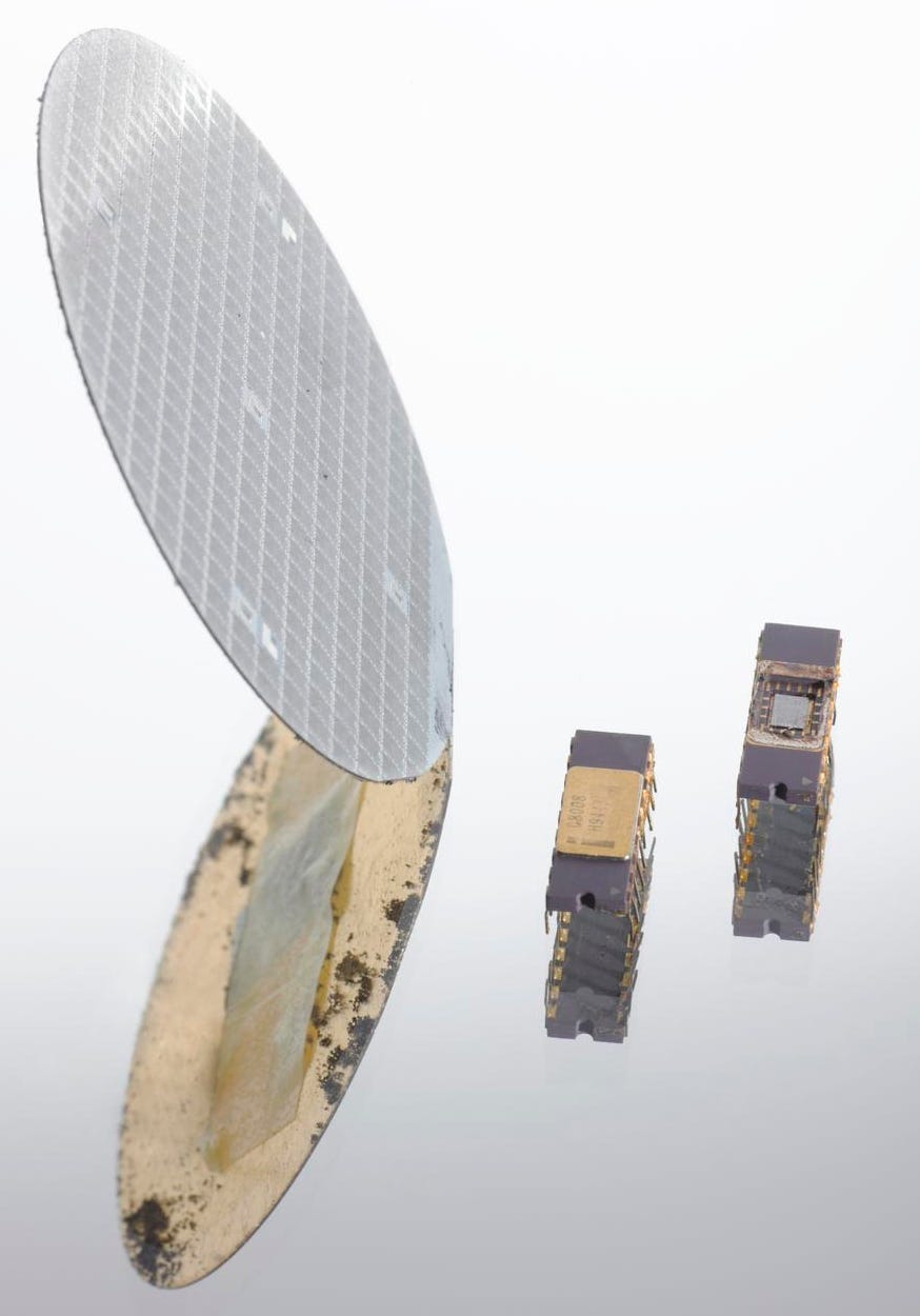
The 8008 was announced to the world in the March 13 1972 edition of electronics magazine, hidden away on page 145 in an article entitled ‘8-bit parallel processor offered on a single chip’. Samples of the 8008 cost $200, more than $1,500 adjusted for inflation today.
In contrast to the full page announcements that had heralded the 4004 it was a low-key introduction to the world. Perhaps, with TI having stolen their thunder, the Intel team felt they had less to crow about.
We’ll see what happened to Intel’s competition and look into the impact of the 8008 in the next post in this series.
July 1968 - Intel Founded by Robert Noyce and Gordon Moore
Dec 1969 - Intel’s Stan Mazor proposes single chip 8-bit CPU to CTC’s Victor Poor
Mar 1970 - Hal Feeney joins Intel and starts work on the 1201/8008
Apr 1970 - Federico Faggin joins Intel and starts work on the 4004
Jan 1971 - Federico Faggin completes work on the 4004 and switches to the 8008
Mar 1971 - Intel starts shipping the 4004
Jun 1971 - Texas Instruments announces 8-bit CPU for the Datapoint 2200
Nov 1971 - ‘Announcing a new era of integrated electronics’ advert for 4004
Mar 1972 - Intel announces the 8008