A few developments since our August 22 issue are worth keeping on your radar.
MiniMax’s business has flipped from consumer apps to APIs and enterprise AI. Open Platform and enterprise revenue rose more than 700% year over year in the first half of 2026 and reached 63.4% of revenue. Read more →
Xpeng Robotics raised more than US$900 million in a first round led by IDG Capital, with Tencent and Alibaba joining as strategic investors. The company says IRON will enter mass production by the end of 2026. Read more →
At the World Robot Conference in Beijing, the more useful questions were becoming mundane: payload, working hours, failure rates, cost and whether a robot can be left on a factory floor. Read more →
Will YMTC’s IPO Mark the Start of a New Global Memory Company? traces Xtacking, Chinese etching equipment and YMTC’s Wuhan fab buildout. A companion to today’s piece.
CNN (August 22, 2026): We joined CNN to discuss China’s humanoid-robot push.
YMTC’s story begins in Wuxi in August 1990, twenty-six years before the company existed. China could assemble increasingly sophisticated electronics but remained hopelessly behind in making the chips inside them, and Project 908 was supposed to close the gap. The state put RMB2 billion (about US$418 million at the time) behind Huajing, operator of Wuxi Factory No. 742, to build a six-inch wafer line and develop the ability to design and manufacture its own chips. It became a centerpiece of China’s Eighth Five-Year Plan for 1991 to 1995.
One distinction matters for the rest of this story. NAND is persistent storage: it holds data when the power is off and goes into SSDs, smartphones and data centers. DRAM is faster working memory that sits closer to the processor but loses its contents without power; HBM, the expensive memory stacked alongside AI accelerators, is a specialized form of DRAM. AI is increasing demand for all three, but in different ways. HBM feeds processors at enormous bandwidth, while NAND stores the training data, model checkpoints and other information that does not need to remain in the most expensive tier of memory.
Huajing produced its first 256-kilobit DRAM in 1993, but the main Project 908 line took eight years to reach production. By then, the imported equipment and manufacturing process were already dated: China had spent heavily on a new fab only to arrive with an old one.
By late 1995, Chinese chipmakers were still at least three generations behind global leaders, a gap one national leader reportedly called “shocking” after touring Samsung’s semiconductor line in South Korea. That November, electronics minister Hu Qili proposed another attempt. At a State Council meeting on December 13, Jiang Zemin said China had to develop integrated circuits even if it meant selling the cooking pots for scrap, while Premier Li Peng gave what became Project 909 special treatment so money could be deployed without the usual layers of review. Hu had identified the problem plainly: the government’s approval cycle was longer than the semiconductor product cycle.
Project 909 became the much better-funded semiconductor centerpiece of the Ninth Five-Year Plan, covering 1996 to 2000. Beijing and Shanghai created Hua Hong, put Hu in charge and made an eight-inch DRAM factory in Pudong the core project, prompting a friend to warn him that he had “put a land mine on his head.” Foreign chipmakers were initially reluctant to provide the missing technology, but Japan’s NEC agreed to a joint venture in 1997. Hua Hong sent its factory workforce to Japan for training and entered production in 1999, with trial wafers reportedly yielding above 50% and yields reaching 90% within three months. The timing initially looked fortunate: Hua Hong caught the end of an industry upswing and was profitable in its first year.
Then memory prices collapsed. By 2002, the global DRAM downturn had left Hua Hong with a RMB700 million (about US$85 million at the time) loss in a single year, and the company eventually abandoned memory to focus on manufacturing chips designed by others. Project 908 had moved too slowly to catch the technology; Project 909 moved fast enough, only to discover that catching the technology was not enough if you could not survive the cycle.
The two projects nevertheless left China with engineers, factories and a much clearer understanding of what it was missing. China’s share of global chip consumption rose from 2% in 1995 to 25% in 2005, even as domestic supply lagged far behind. The foundry model proved more forgiving: SMIC began volume production in 2002 and became the country’s largest and most advanced foundry, but China still had no domestic memory champion. A foundry could manufacture chips designed by other companies; a memory producer had to continually develop its own products, raise manufacturing yields and drive down the cost of every bit before the next price collapse. That was proving to be a much harder institution to build.
While Hua Hong was getting out of DRAM, Wuhan was trying to push East Lake’s “China Optics Valley” beyond optical fibre and telecommunications equipment. The city began courting chipmakers around 2000 and had plenty of the ingredients for a semiconductor industry — universities, research institutes and electronics companies — but no large wafer fab. That was a critical omission. A fab is where circuits are physically built, layer by layer, on silicon, but it also concentrates the process engineers, equipment qualification, materials suppliers and production knowledge that designers and electronics assemblers cannot develop on their own. Without one, Wuhan could design and assemble increasingly sophisticated electronics while leaving the hardest and most valuable part of production elsewhere.

In January 2006, Hubei named integrated circuits as one of the province’s three emerging electronics chains, fitting neatly with Beijing’s campaign, launched in 2004, to push more advanced industry into central China. Hubei, Wuhan and the East Lake development zone effectively treated the proposed fab as industrial infrastructure, committing RMB10.7 billion, about US$1.34 billion at the time, to Wuhan Xinxin, or XMC, with support from China Development Bank. Wuhan could pay for a factory, but it could not yet run one, so SMIC, already China’s largest and most advanced domestic chipmaker, agreed to operate it. The arrangement was straightforward: the local state would take the capital risk, while an experienced outside operator supplied the manufacturing knowledge money alone could not buy.
The planned 12-inch line, using 90-nanometre and smaller processes, was eventually supposed to produce 20,000 to 25,000 wafers a month across logic and memory products. The investment amounted to nearly one-tenth of all state-sector investment in Hubei that year, and Wuhan’s industrial plan made clear that the fab was only the beginning. Chip designers, equipment and materials suppliers would come first, followed by packaging, testing and product companies. In effect, the city was buying the nucleus around which an industry could form.
It nearly failed anyway. XMC began production in September 2008 just as the financial crisis hit, with initial capacity of only about 3,000 wafers a month against the planned 20,000 to 25,000. One industry expert told China Business News that a 12-inch fab generally needed at least 30,000 wafers a month to break even. XMC found work producing flash memory for Spansion, formed from AMD and Fujitsu’s flash operations, only for Spansion to enter bankruptcy protection the following year and its orders reportedly disappear. TSMC came close to a deal with Wuhan before regulators withheld approval, and by 2010 Micron was discussing an investment and possible control of the factory. Wuhan chose to keep it.
As a business, XMC had hardly justified its original investment. But closing the factory or surrendering control would have meant losing the engineers, supplier relationships and production experience Wuhan had spent years assembling. An underused fab was expensive to maintain; rebuilding that ecosystem later would have required another cycle of construction, recruitment, qualification and trial production. XMC’s value was ultimately less in what it produced during those early years than in what it preserved: Wuhan’s place in the semiconductor industry until national policy and capital caught up.
By 2014, Beijing had spent two decades learning what it took to build a competitive semiconductor manufacturer. Project 908 reached production with technology already dated; Project 909 moved faster, but Hua Hong’s DRAM business could not survive the collapse in memory prices. The national integrated-circuit guidelines issued that June took a broader approach, putting manufacturing at the center of a domestic supply chain spanning chip design, equipment and materials, while emphasizing scale and consolidation. In September came the first phase of the National Integrated Circuit Industry Investment Fund, better known as the Big Fund, which could take equity stakes in semiconductor companies rather than simply finance individual production lines.
Memory remained a conspicuous gap. China was already the world’s largest market for many electronics products, but advanced DRAM and NAND came from a handful of foreign suppliers. Staying competitive required repeated investment in new generations while continually lowering the cost per bit. Beijing wanted a company with enough capital and scale to keep investing through both technological transitions and industry downturns.
China’s 2016 memory push also produced a division of labor rather than several state-backed companies chasing the same technology. YMTC in Wuhan pursued 3D NAND, while CXMT in Hefei and Fujian Jinhua focused on DRAM. Jinhua’s effort later stalled following a legal dispute and US restrictions, leaving CXMT as China’s large-scale DRAM producer and YMTC as its only advanced 3D NAND producer operating at national and global scale. We wrote about CXMT, and the very different path China took to building its DRAM champion, in detail earlier this summer. CXMT has since become China’s most valuable listed company by market capitalization. (You can read more about it and the overall Chinese chip sector at our Chip Tracker.)
XMC’s difficult first decade now worked in Wuhan’s favor. A person involved in the later site-selection discussions told Times Weekly that the city’s industrial base was considered “relatively clean”: no foreign memory giant controlled a local fab, while XMC provided a decade of engineers, equipment and production experience. In 2016, the planned RMB160 billion (US$23.6 billion) National Memory Base was assigned to Wuhan, then the largest single high-technology investment project Hubei had undertaken.
YMTC was formally launched on July 26, 2016, using XMC’s existing production base. Tsinghua Unigroup provided the corporate platform, the Big Fund and other state vehicles supplied capital, and Hubei and Wuhan contributed the fab, workforce and local network. Chairman Zhao Weiguo, who had been at Tsinghua Unigroup, promised a “larger funding platform, stronger execution and faster development.” Xinfei Technology, the Big Fund, Hubei Science and Technology Investment and Guoxin Fund contributed cash and stakes, and by early 2017 the new parent had registered capital of RMB38.6 billion (US$5.69 billion). Unlike the earlier projects, the state had created a company that could keep deploying capital as the technology changed.
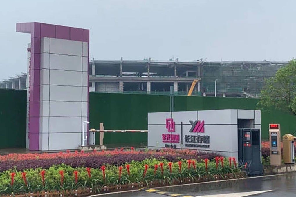
Capital did not eliminate the technological gap. When YMTC was established, Samsung was already three generations into vertical NAND and preparing its 64-layer generation for production. YMTC completed its first 32-layer chip in 2017 and began limited production the following year, but CEO Yang Shining acknowledged in 2018 that its costs were not competitive. Rather than increase output of the mature 32-layer product, which he said would have been easy, YMTC kept volumes small and focused on 64 layers. This was an economic decision as much as a technical one. NAND prices fall as suppliers pack more bits onto each wafer; producing an older design successfully does little good if every bit costs more than the market will pay.
Yang also emphasized that YMTC intended to compete through its own technology. Products, he said, went through 500 to 1,000 experimental runs before passing. At the same conference, amid concerns that state-funded Chinese capacity would worsen the NAND downturn, he insisted that YMTC had come “to make money” and was “not here to wreck the market.” The remarks, recorded by CFMS and DIGITIMES, reflected the two things YMTC needed to prove: that it could innovate technically and compete commercially without relying indefinitely on subsidized capacity.
Xtacking became the clearest expression of that strategy. Developed under technical leaders such as Huo Zongliang, the architecture manufactures the memory array and peripheral logic on separate wafers before bonding them together. The two parts can therefore be developed in parallel and optimized for different processes, an advantage for a late entrant trying to close the gap quickly. YMTC says the approach cuts product development by at least three months and the manufacturing cycle by 20%, although it also makes the final bonding of billions of microscopic connections critical to production yield.
YMTC unveiled Xtacking at the Flash Memory Summit in Silicon Valley in August 2018, just two years after its founding, and won the conference’s Best of Show award for the most innovative flash-memory startup. Huo later called it “a new flash-memory path of China’s own.” By 2022, Xtacking 3.0 supported a 232-layer, one-terabit chip, putting YMTC among the first manufacturers to ship NAND with more than 200 layers.
Commercial validation appeared close. In March 2022, Reuters reported, citing Bloomberg, that Apple was testing samples of YMTC’s NAND. A company built on the remains of a struggling Wuhan fab was approaching the supply chain of one of the world’s largest consumer-electronics companies.
Then the window closed. On October 7, Washington imposed new restrictions on equipment and support for Chinese fabs producing NAND with 128 layers or more, putting YMTC’s advanced production directly inside the policy boundary. Reuters reported later that month, citing Nikkei, that Apple had put its plans on hold. In December, BIS added YMTC to the Entity List, subjecting covered exports, reexports and in-country transfers to stringent licensing requirements.
The restrictions threatened more than YMTC’s ability to buy new machines. Advanced fabs depend on replacement parts, software, process recipes and engineers from equipment suppliers to improve yields and introduce new generations, making localization an operating requirement rather than simply an industrial-policy goal. YMTC nevertheless put Xtacking 4.0 products into volume production in 2024, and Reuters reported this April that Chinese suppliers provided more than half the equipment ordered for its third Wuhan fab, including critical tools used to manufacture vertical NAND stacks.
The IPO filing brings the story to a remarkable point. Its fifth-generation products are in volume production, with a sixth generation under development, and its factories ran at 98.02% utilization in the first quarter of 2026. Based on TrendForce data cited in the prospectus, YMTC ranked third globally that quarter in both NAND sales and shipments. Revenue reached RMB47.04 billion (US$6.93 billion) in just three months, nearly three-quarters of its entire 2025 total.
Weijin Research, a TBC partner whose work we help publish, argues that the nature of 3D NAND helps explain why YMTC has been able to keep advancing under export controls. Unlike leading-edge logic, 3D NAND does not require EUV lithography. One of the key challenges instead is high-aspect-ratio etching, which cuts extremely deep, narrow channels through an ever-growing stack of memory layers. Weijin argues that advances by Chinese etching suppliers led by AMEC, together with YMTC’s Xtacking architecture, have given the company a workable domestic path to denser chips and more capacity despite restrictions on foreign equipment and support.
How far that can take YMTC is less certain. Weijin estimates that a full five-fab buildout in Wuhan could push its global NAND share above 20%, making it the world’s second-largest producer, and sees a longer-term possibility of adapting Xtacking to 3D DRAM.