(Note: this entire post is my opinion)
“Substrate” has been in the news for allegedly coming up with a way to make computer chips for much cheaper and at much higher quality than anyone else in the industry.
There’s just one problem: all signs indicate that the entire business is fake.
The founder is a known con artist involved in such other things as solving nuclear fusion and stealing $2.5M in a Kickstarter scam.
The cofounder is the founder’s brother and has literally zero documented professional or academic experience.
The company’s job postings are nonsensical and AI-generated.
The company is unwilling to evidence any of its (extremely extraordinary) claims, which have been made on a timescale that makes no sense in the context of the semiconductor industry.
The company’s research facility is, based on photographs that they’ve published, at least two orders of magnitude smaller than what would be necessary.
There’s a lot of money to be made in making computer chips. So, a natural question to ask is, “how are chips made?”
There is no one person in the world who knows the full answer: even small parts of the process can represent the work of a thousand experts. At a high level, though, it looks something like this: a company, called a foundry, makes them at a fab, where they get a big, circular wafer on and with which many transistors and wires will be built. Many chips will be built on one wafer (though “wafer-scale” chips do exist) and they will be separated and packaged at the end.
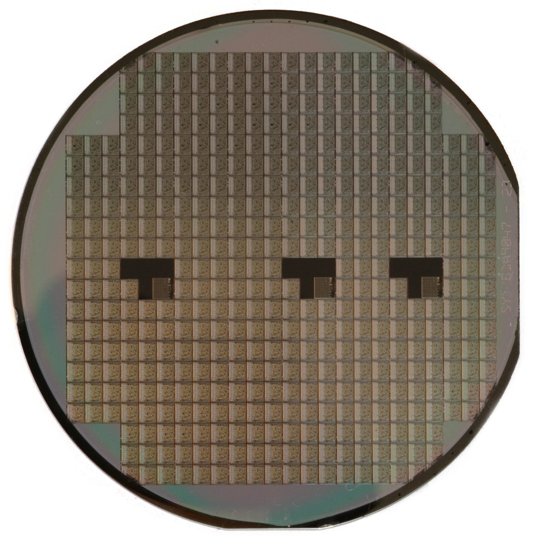
(Photo of a wafer. Credit: Inductiveload on Wikimedia.)
.jpg")
(Close-up photo of a chip taken off of a wafer. Credit: Fritzchens Fritz.)
There are two relevant ways of actually creating the patterns of wires and transistors that make up a chip; the first is like writing them with an ink and quill, where you directly write the patterns by some means. The second is like using a printing press, where you either physically imprint a chip with a pattern (nobody uses this despite Canon’s best efforts) or use high-energy light through a patterned mask.
Chips can have a very large number of layers, so if this were all done using the ink-and-twill “direct write” method, you would have no chance of manufacturing trillions of transistors every second. Unfortunately, that is exactly the throughput that is expected from fabs. Worse, directly writing onto a wafer is very hard to do consistently: imagine writing any letter perfectly a trillion times.
“Scanning,” the method used by Substrate’s competitor, ASML, is the approach that uses the patterned mask. ASML gave “EUV” scanning machines to a foundry named TSMC in 2014. It took 5 years and billions of dollars in yearly R&D spending before TSMC was able to use it in high-volume manufacturing, even with TSMC having decades of experience with ASML scanning equipment.
There are ways of speeding up the direct writing method, but nothing particularly relevant; for example, the masks used in ASML’s scanning machines can be produced by e-beam lithography machines. Because masks are in such high demand, IMS Nanotechnology’s mask-producing machines use multiple e-beams in parallel to increase throughput. Nevertheless, throughput is still several orders of magnitude below scanning machines’.
Finally, it is important to note that the smaller the patterns can be, the more wires and transistors you can write—which is great—but the longer it takes to direct-write a full wafer, which is part of why nobody tries. This is much less of a problem with scanning.
Accordingly, if someone claims to be using a direct-write approach to lithography for high volume manufacturing, you should be very, very skeptical.
Despite claiming to be competing with a $400 billion dollar company and despite being strapped for cash in an industry where technology is the only sustainable way to raise funds, Substrate does not talk about their technology, other than to say that they use X-rays. Fortunately, SemiAnalysis has shared pictures from Substrate of “test patterns” that they etched onto wafers.
You can read their article below:
In SemiAnalysis’ post, Substrate claims to have properties that are massively better than what ASML is capable of doing. Such extraordinary claims—ASML has worked on their technology for decades, spending billions per year, and Substrate has raised less than $100M—might make sense if they were directly writing patterns. And indeed, from the images they’ve shared with SemiAnalysis, there are clear tells that this is exactly what they’re doing: for one, the lines are just…strange. First, the picture Substrate provided:
")
Now, look closely:
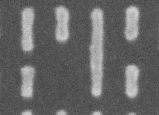
There is a lot of spacing between lines and a lot of variation in width inside lines. What can explain this?
Well, in e-beam lithography (and with other direct writing methods, but e-beam is the best-documented), you have what are called write subfields, and in those, you can describe the shapes you want to see the machine write, where (not) to apply energy to the substrate, etc. You can imagine it like a printer where you have a fixed number of dots-per-inch. Spacing between lines can’t be that much smaller than the lines themselves.
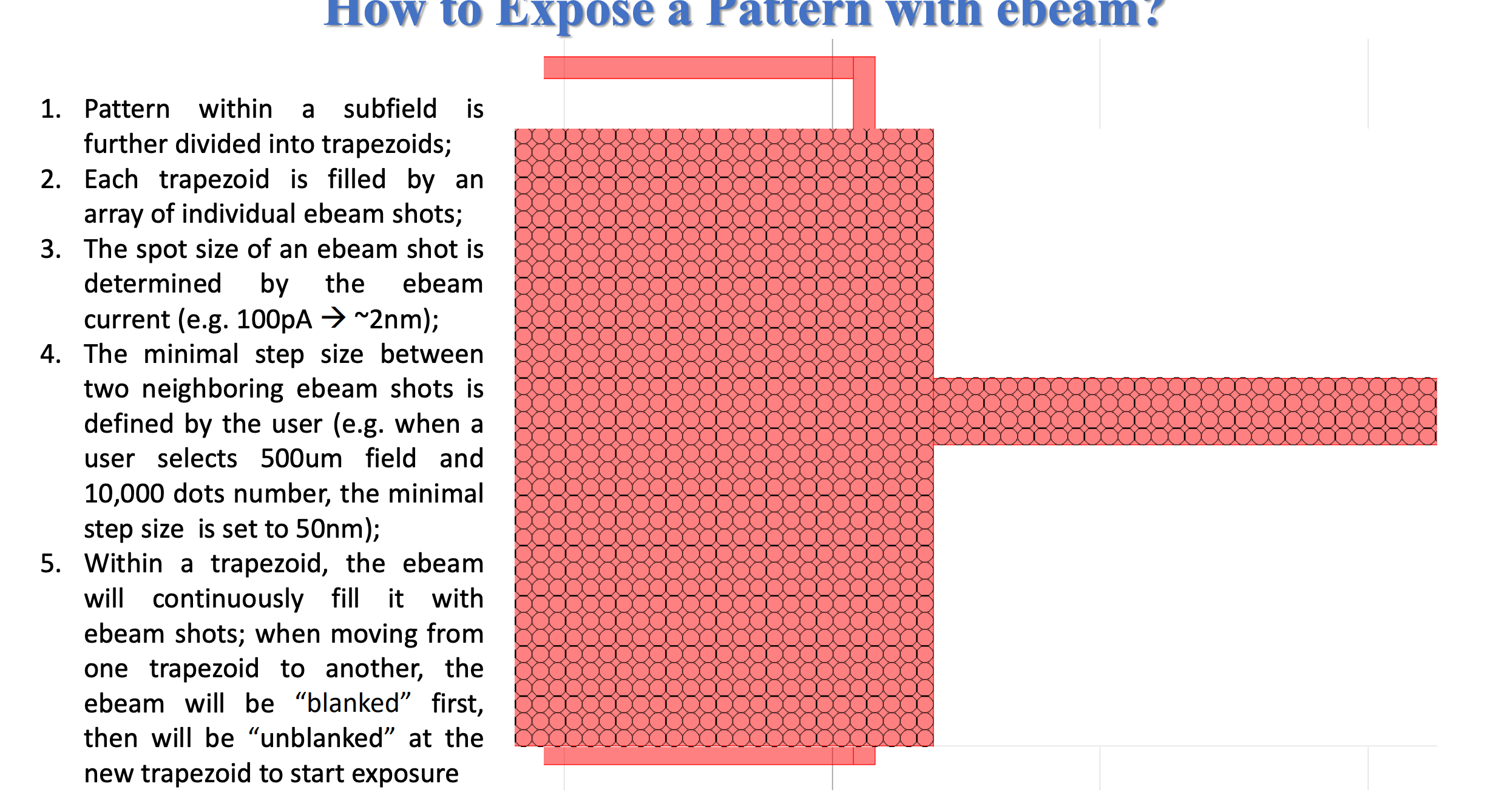
(Source: University of Wisconsin)
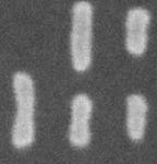
This means you tend to get fairly wide (line-width), uniform spacing between exposed and unexposed areas. Compare to the lines created by ASML’s scanners (hat tip: Andreas Schilling):

There’s very tight spacing with ASML’s patterns. Further, because it’s not being written as if by a pencil, the lines all have nice, stencil-like uniformity. To be clear, this is not damning or proof that direct-writing was used; however, it is strongly indicative that this is a maskless approach to lithography.
There’s an additional red flag: while they told SemiAnalysis they could do very narrow feature sizes, SemiAnalysis does not state that this is a picture with those feature sizes, and there is no annotation on the image to indicate that they used narrow features.
And if it’s direct-write, then this is not any different from what many university students have done for years.
Lithography research needs to take place in large, extremely high quality clean rooms: think acre upon acre of extremely high-purity environments.
Substrate has a small, informal box smaller than plenty of lithography machines.

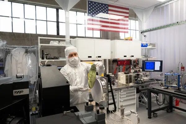
(Source: Reuters)
The company’s founders are James Proud and Oliver Proud. Neither have any background in the semiconductor industry. Neither have any professional work experience whatsoever, nor have they attended college, conducting a total of zero hours of postdoctoral work into next-gen X-ray lithography, which is infinitely many orders of magnitude less than the millions that have been spent so far without any fruit.
James Proud’s last project was a Kickstarter scam. It raised $2.5 million dollars for an alarm clock that did not function as advertised, and that—despite a flashy marketing effort—did not actually do anything it was marketed as doing when the Kickstarter launched; rather, it was a con. While, after $40M in funding, it was eventually able to ship hardware, the hardware did not live up to expectations.
From The Verge:
When I reviewed the Sense sleep tracker and described it as only marginally better than a sham product, I felt bad. Time has now validated my assessment, as Hello Inc, the company built around the Sense tracker as its sole product, is going under — but I still feel bad.
The person announcing the shutdown of Hello, James Proud, is the young founder of a small team that led the company and its sleep-tracking gadget through a successful $2.4 million Kickstarter campaign, $10.5 million in Silicon Valley funding, and a subsequent $40 million funding round. More than 19,000 backers bought into the Sense idea, so it was clearly hitting on a hot area of consumer interest and demand, however the one thing the company forgot to do was develop a robust device that actually did what it promised.
What bums me out about the entire Sense saga is how calculated the whole thing felt and still feels. Proud was one of Peter Thiel’s entrepreneurial fellows, which is a scheme the Facebook board member initiated to get young people to skip university for a $100,000 grant to pursue some business idea and put their skills to practical use. My impression is that the idea with Hello, in classic Silicon Valley style, was to tap the most underserved market — there’s been plenty of data to show that sleep diagnostics has been a big and underdeveloped opportunity — and just figure out the product along the way. Needless to say, neither the “let’s do a startup and figure out the hardware later” nor the “let’s build a device and figure out the business aspects later” attitude is the right one, but the idealist in me leans more toward the latter approach. I know of more companies, such as YouTube, that have turned a popular but unprofitable product into a viable business than I know of companies that developed good products after their slick marketing campaign.
While they took $2.5 million from 19,000 buyers for their largely non-functional $149 smart alarm clock, which took years to be built and delivered; a further $10.5 million from investors; and another $40 million from even more investors (adjusted for inflation, this is about two-thirds of what they’ve raised for their fab), they seemed to have burned through it rather quickly. Indeed, according to the BBC, there were no refunds:
Customers have been told that the company is “unsure” whether the online service that supports the hardware will continue to operate - it would need to be acquired by a third-party. But they can export their existing data.
Owners have also been advised to request refunds from shops they bought the devices from.
However, if they purchased the kit directly from Hello itself, they have been told there will be no way to get their money back.
Buyers were also told they could use their own API for the tracker so that the device could still be useful if servers were ever shut down. This was also untrue.
Surprisingly, the founder of the scrappy startup behind that smart alarm did not seem to struggle to the same degree financially; he still owned his $1 million San Francisco condo in 2022 and appeared able to live off of the money from this Kickstarter scam.
For reasons possibly related to the nepotism involved in the company’s creation, the founders do not know what they are hiring for. Their job postings, in fact, are entirely fake, and were created with an LLM that, seemingly, they asked to come up with roles for a foundry that is doing everything in-house. This has given way to genuinely funny job postings; for example, an electromechanical engineer whose job it is to design chucks.
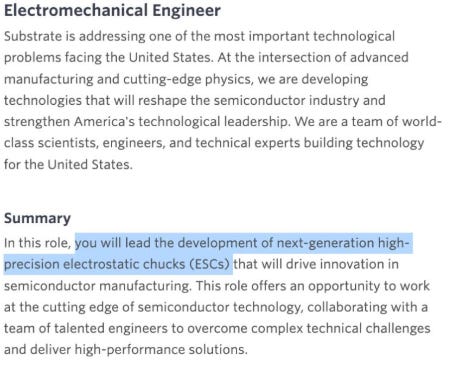
These are extremely cheap but would take a very long time to do right “in-house”—it’s like starting a small pizza business and making your first job listing “invent and manufacture a new type of automobile to allow employees to arrive at customer locations.”
Likewise, they have another job posting for a cell design lead.

This does not make sense because they only have one location and the detailed requirements of the job posting require years more progress before it’s possible for a cell design expert to be able to actually do anything. It’s like creating a motorsports job posting before the internal combustion engine. Again, it makes no sense.
Unless my claim about their use of an LLM is true. And…

As it turns out, it is true. This strongly suggests they do not have the talent or ability to acquire talent that would be necessary to do what they’ve claimed.
For one of the most capex-intensive industries in the world, you would expect more transparency about their accomplishments, as it’s the most effective way to raise money: people want to invest in good tech, so if you have the best tech, why not show it? ASML is a near half-trillion dollar business for a reason.
Con artists tend to rely on confidence, rather than evidence, to make their pitch. And we see that with James Proud, the founder.
Would you believe that the founder—who could not make an alarm clock for $70 million, but who has allegedly beaten ASML for under $100 million—has also found time to try to solve nuclear fusion?
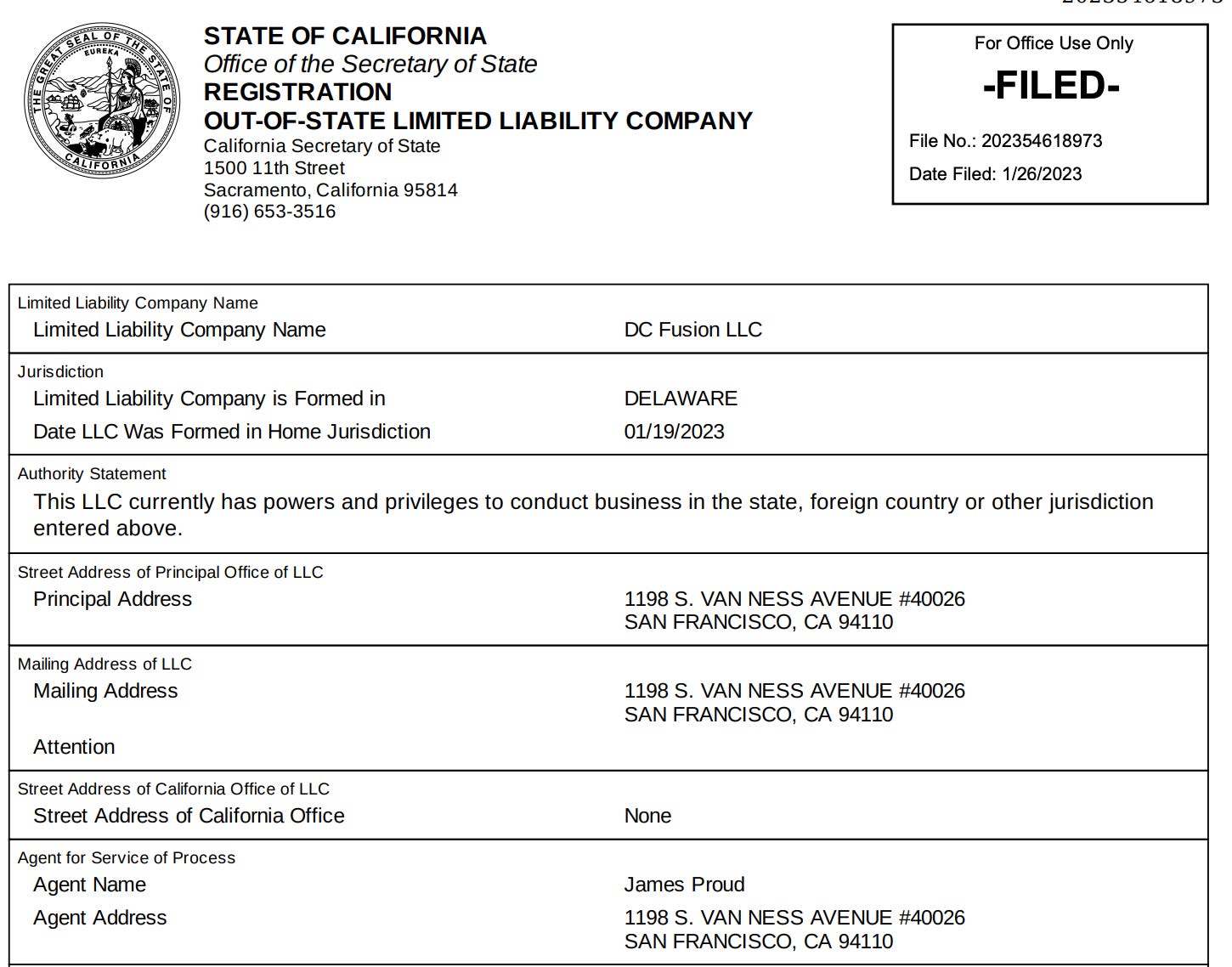
Because the same PO box and name associated with Substrate is also associated with a fusion startup.
Would you believe that, with the best technology in the world, they are totally unwilling to share any concrete evidence of their technology’s existence with anyone? Substrate claims they will “reduce the cost of leading-edge silicon by an order of magnitude compared to the current cost-scaling path we are on. By the end of the decade, Substrate will produce wafers closer to $10,000, not $100,000.” This is a remarkable claim, but rather than evidence it, Substrate’s founder seems to point to his investors, American dynamism, and politicians for reasons to believe in the company.
It’s noteworthy that none of those things saved his last startup nor the customers that it robbed. (Though, in fairness, they did save his condo.)
Because Substrate’s founder repeatedly points to his investors as a sign of trust, it’s worth considering that maybe their investors are smart and see something I don’t. However, I don’t believe that’s the case:
Suppose this were all real, and a known con-artist with zero knowledge of semiconductors was able to transform the industry for under $100 million, in a tenth of the time and roughly thousandth the cost that it took to make EUV work. It stands to reason, then, that the Taiwanese, with all of their experience and expertise, preexisting fabs and packaging plants, client relationships, cheaper labor costs, extensive knowledge pools, etc., could replicate the feat in a fraction of the time, then blow past Substrate in scale and sophistication shortly thereafter. Domestically, Intel—an American company—could do the same, if somewhat slower than TSMC, so national security arguments would not save Substrate.
ASML’s singular moat is that catching up to them is believed to take tens of billions of dollars, if not hundreds of billions. Substrate’s claim is that they did this all with under $100 million. Accordingly, as an ASML competitor, Substrate does not have ASML’s moat. Maybe Substrate finds a way to wield patents, but watertight manufacturing process patents are impossible in a field like semiconductor manufacturing, and the Chinese foundries certainly would not care about patent infringement. Semiconductor analysts and investors would know that Substrate has no moat and would be eaten alive.
Accordingly, you should expect Substrate to seek naive investors from outside the semiconductor industry, and whose judgement would be less relevant or credible within it. You might also see Substrate try to attract smaller investments but from more investors in order to attract less scrutiny from each.
Well, their funding is almost exclusively from a large number of firms, none of which are highly involved in the semiconductor industry.
From DatacenterDynamics:
The company also announced it raised $100 million in a funding round, which valued it at $1 billion. The round saw participation from Peter Thiel’s Founders Fund, General Catalyst, Allen & Co., Long Journey Ventures, Valor Equity Partners, and the CIA-backed not-for-profit firm In-Q-Tel.
This confirms that Substrate’s fundraising attempts reflect behavior that attempts to exploit more naive investors. Accordingly, you should not be relying on the judgement of their investors as a reason to believe in the company.