“Quantity has a quality of its own.” - Joseph Stalin
“Hardware failures won’t limit AI scaling.” - Epoch AI, i.e. no square-cube-law type limitations for AI training as AI clusters grow in size and number of components.

How Constraint Becomes a Design Philosophy in Nature and in GeoTechnical Competition
During his 1835 voyage on the HMS Beagle, Charles Darwin collected several small bird specimens from the Galápagos Islands, initially misidentifying them as unrelated wrens, blackbirds, and mockingbirds. It was only after returning to England that ornithologist John Gould revealed these birds were actually a collection of closely related, unique finch species. This critical realisation directly inspired Darwin's radical new idea of the "theory of evolution." He deduced that a single mainland ancestor had colonised the islands, with its descendants gradually branching out into entirely new species to survive. The most striking evidence of this was their highly specialised beak shapes, which had evolved via natural selection to match specific food sources, from crushing hard seeds to probing cactus flowers (Decades later, modern researchers Peter and Rosemary Grant confirmed this theory on the island of Daphne Major, documenting real-time evolution as droughts and rainy seasons rapidly altered the finches' food supply and drove measurable changes in beak sizes.).
This is what isolation does to evolution. It does not just weaken isolated species; it pushes them in new directions. Free from mainland competition and shaped by local constraints, island species evolve along paths the wider world does not take. The results can look strange or inferior by general standards, but they are well adapted to their specific environment.
Huawei is in a similar position. Export controls are its isolation: no EUV lithography, no leading-edge process nodes, no unrestricted HBM. Rather than building an inferior copy of Western chips, Huawei has developed in a different direction, optimising for what its environment allows. While Nvidia and AMD focus on transistor density because they have access to advanced silicon, Huawei has had to ponder over a different question: what can you build into a world-class AI system when you cannot have the best transistor density? The answer is quite a lot actually, if you are willing to use the resources you do have—power, space, mature manufacturing, and strong communications technology—to compensate for the one you lack: transistor density. That is the subject of this essay.
Because EUV lithography will remain unavailable for the foreseeable future, Huawei has focused on areas where transistor density is not the deciding factor. Its approach, described in what it calls the Tau scaling laws, is to scale along the time dimension: if you cannot keep making each die denser and faster at the historical rate, you improve connectivity to reduce time delays. Huawei is applying this idea not only to chip design, which has been covered widely in the media, but also to systems: networks and overall AI cluster design. That system-level work is the topic of this essay. The second version of the τ-scaling paper describes three coordinated layers that reduce system latency together:
a unified system fabric (UnifiedBus, or UB),
a near-packaged optical engine (Hi-ONE), and
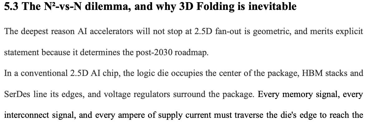
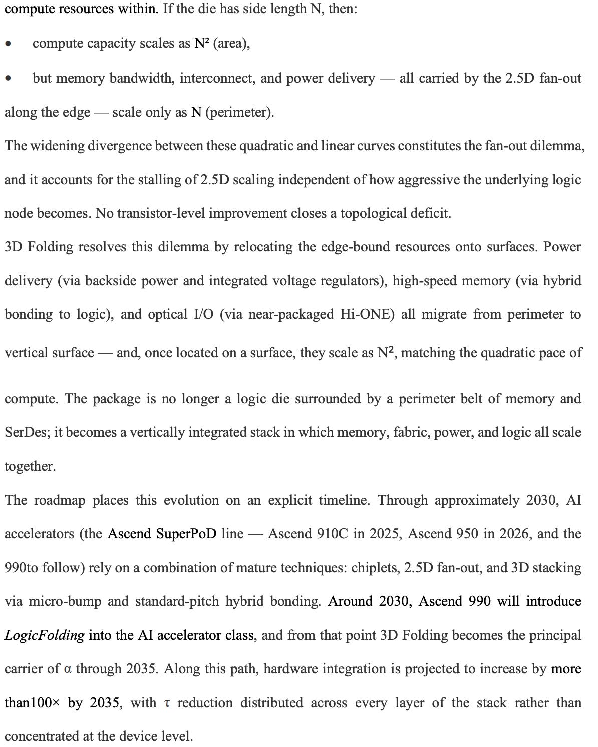
a reorganisation of the package topology (3D Folding, which turns a quadratic scaling problem into a linear one by moving edge-bound resources onto surfaces).
The goal of this stack is a large-scale AI cluster that works as a single logical unit, which Huawei calls “System-as-One-Chip.”
Evolution is unplanned, but Huawei’s adaptation is deliberate. The Galápagos finches did not choose their beaks; they stumbled into those shapes due to evolutionary pressure. Huawei’s engineers, on the other hand, are treating their constraints as design guidelines and rapidly trying out ideas that will meet or overcome those constraints. What nature reaches over millennia through trial and error, a focused company can engineer within a few product cycles. This essay is a story of that adaption…
The instrument of this strategy is the Unified Bus (UB) now in its version two: it replaces need for having different protocols like NVLink, PCIe, Ethernet etc.
It is Huawei’s approach to networking AI data centers. They have two version of it: 1) Flat/CLOS: as implemented in CloudMatrix 384 (384 Ascend 910s), 2) UB-Mesh which is a 4D-FullMesh with CLOS for PoD level networking for training.
Various sources indicate Ascend 950 based SuperPoDs have multiple topologies possible flat/CLOS for inference, as well as, hybrid involving UB-Mesh for training. -
The flat/CLOS need more switches and more optical interconnects (NPO, we will see more about it later), hence costs more for networking, but is ideal for implementing inference topologies like WideEP with large model.
UB-Mesh (nD-FullMesh + CLOS) reduces need for switches and optical interconnect. It in-fact costs less than 1/3 of flat/CLOS topologies. It takes the advantage of the fact that most traffic during training is local/is within groups of nodes and NPUs.
Confirmations on Ascend 950 supporting both:
You can learn more here about UB-Mesh: a Hierarchically Localized nD-FullMesh Datacenter Network Architecture published in March, 2025. In addition to UB-Mesh, which is a specific topology (nD-FullMesh + CLOS), you will learn about UB design philosophy in general. The Ascend 950 Architecture paper and Tau Scaling Laws V2 paper published in Jun 2026 add more details.
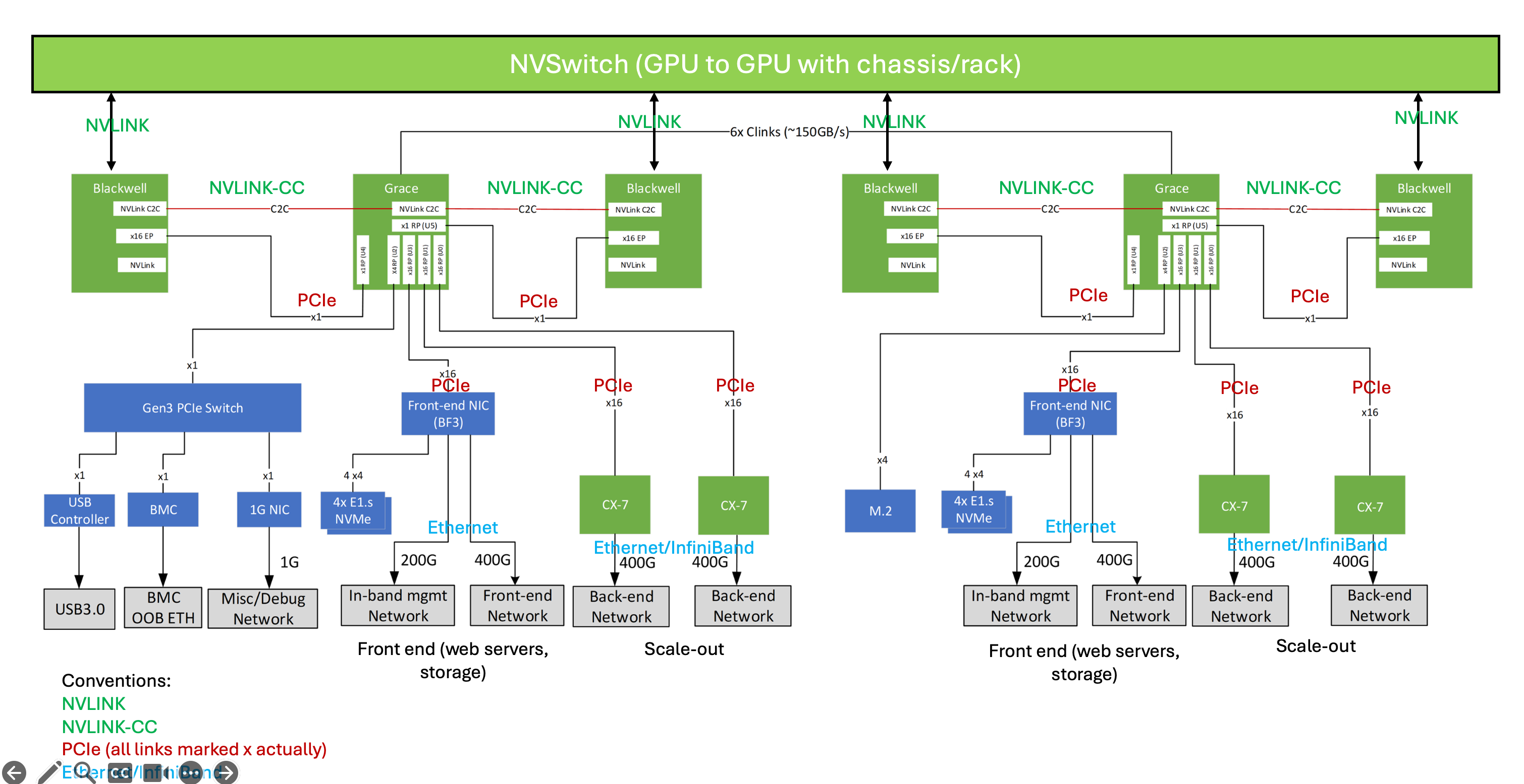
Prevailing architectures move every byte through layered protocols - PCIe to the host, a proprietary fabric in the chassis/rack, Ethernet or InfiniBand between chassis/racks, software-managed remote memory on top - and each layer exacts a conversion, a serialization, a buffer, a handshake. Just count how many different network protocols you see around GB200 in the below diagram. Network protocols are color coded.
Here is a great diagram from the UB Mesh paper that explains distinction between the prevailing approach and that of Huawei’s UB:
The paper’s measured result is end-to-end remote access falling from the tens of microseconds of TCP/IP-class stacks to roughly 100 nanoseconds - about a 500-fold compression of system τ along the dominant communication axis. At rack scale the system approaches what the paper designates a System-as-One-Chip: a fabric-coherent machine in fact, not metaphor.
As we saw, where the industry maintains a zoo of interconnects - PCIe between GPU, host & NICs, a proprietary scale-up fabric, InfiniBand or Ethernet for scale-out - UB is a single protocol that carries all of these roles: memory semantics, IO semantics, and network semantics on one wire, with ports flexibly assigned between chip-to-chip and node-to-node duty.
The Ascend 950 exposes eighteen ports (4 links each, totalling 72 total) from one SerDes pool; four can run PCIe, two can run Ethernet, and all of them speak UB natively. There is no seam in the protocol between “inside the rack” and “outside the rack.” Stay with me if it is not clear yet!
Huawei is moving to near-package optics (NPO) and linear-drive optics that eliminate the power-hungry DSP of conventional pluggable modules - leaning on its heritage as a communications-equipment company to do so. From Ascend 950 generation, they use NPO for inter rack/cabinet networking.
Consider why an NVL72 looks the way it does. NVIDIA’s GB200 racks pack seventy-two GPUs into a single dense enclosure not to save floor space but because passive copper cannot carry NVLink-class bandwidth much beyond two meters. Inside that copper tether, each GPU enjoys eighteen NVLink connections at roughly 900 GB/s per direction. Outside it, the system falls off a cliff: scale-out runs over one or two 400 Gbps optical links through discrete NICs - the optical network is, ironically, the slow one.
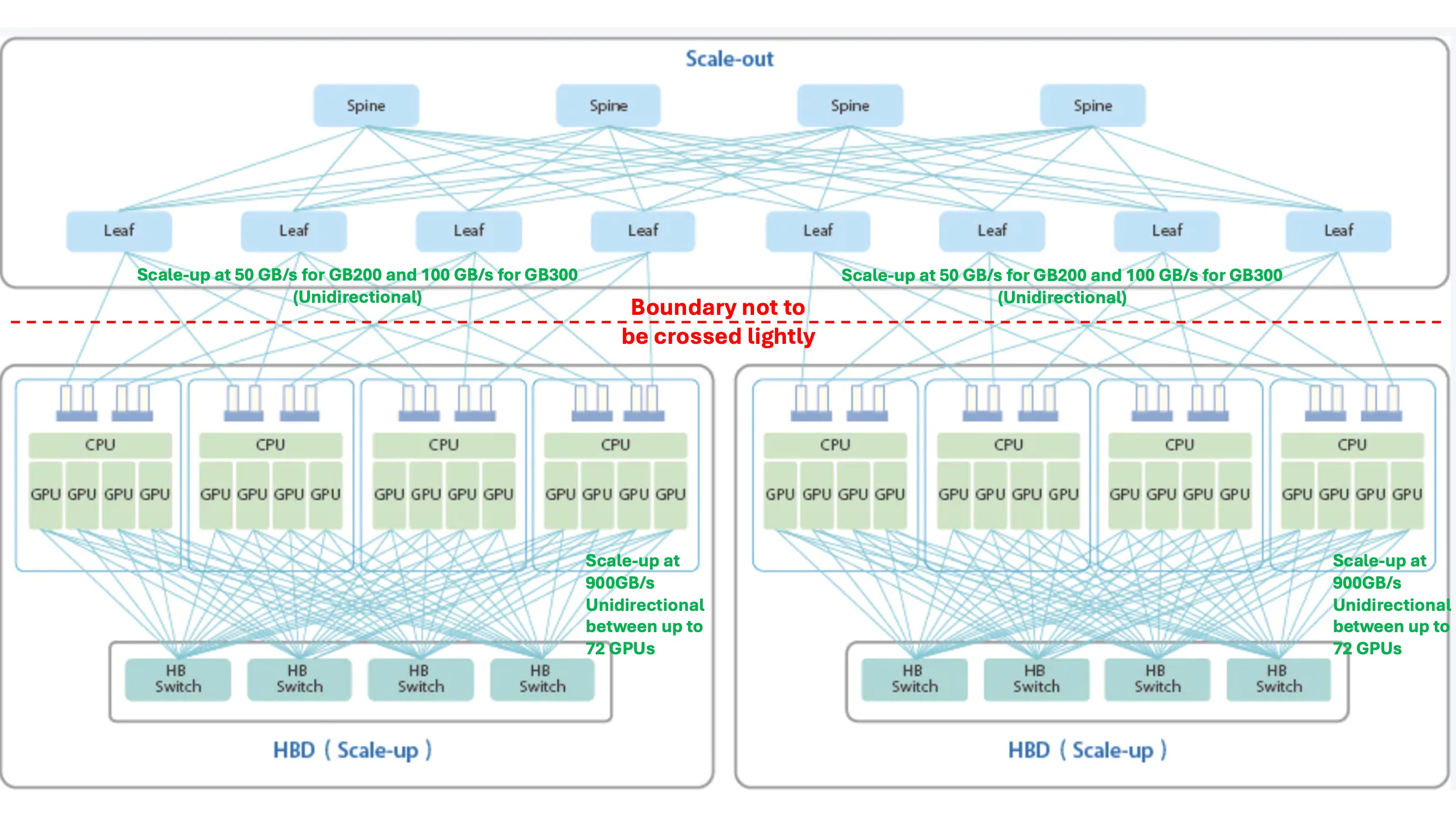
A GB200 GPU speaks to its seventy-one NVLink neighbours at 900 GB/s per direction, and to everyone else at 50 GB/s through a 400 Gbps (50 GB/s) NIC - an eighteen-to-one drop. GB300 softens the fall to nine-to-one by doubling the NIC to 800 Gbps (100 GB/s), but a nine-fold penalty is still harsh. Every large-model parallelism strategy on NVIDIA hardware is, at bottom, an exercise in designing around this ratio: tensor parallelism must stay inside the 900, data parallelism is exiled to the 50, experts are placed with the seam in mind, and much of the framework engineer’s craft is the art of never letting chatty traffic wander onto the thin side of the wall. The result is a two-tier world with a hard seam: blistering bandwidth for seventy-two devices, an order of magnitude less with everyone else. Below diagram presents a simplified network diagram for understanding scale out and scale up, though it doesn’t show 72 GPUs per rack for simplicity.
Huawei’s approach dissolves this geometry, particularly in FLAT/CLOS topology. An Ascend 950 presents 2,016 GB/s bidirectional, just over a terabyte per second each way, from one fungible pool of eighteen ports - whether the peer sits in the next slot or eight rows away. There is no eighteen-to-one cliff to design around, and the developer is spared most of the judiciousness NVIDIA’s ratio requires. The one boundary that remains is semantic still, not bandwidth: direct UB Memory (NVLink equivalent) load/store spans only 1,024 NPUs - the 128 TB address window - while URMA (RDMA equivalent), the asynchronous mechanism that collective communication (NCCL equivalent) actually uses, runs uniformly across all 8,192 NPUs of a SuperPoD (eight rows of sixteen racks/cabinets) and beyond it over UBoE (UB over Ethernet).
If implemented with flat/CLOS, the magic in Huawei’s numbers is this: its everywhere-bandwidth roughly equals NVIDIA’s inside-bandwidth (scale up with NVLink) - and exceeds NVIDIA’s outside-bandwidth (scale out with NICs) ten- to twenty-fold. In case of Nvidia, NVLink uses copper and scale out network (Ethernet of Infiniband) connections use optical transreceivers. For Flat/CLOS topologies, Huawei uses NPO optical links for Ascend 950 SuperPoDs, and optical transreceiver for Ascend 910 based CloudMatrix 384 (while within a rack, CPU and NPUs use copper UBLink to talk to each other via local UB-Switch. NPU-NPU communication happens through a FLAT/CLOS network through an optical link. It costs to use optical links, but that is the trade off you do for ‘flatness’).
SemiAnalysis does an exceptional job of describing such FLAT/CLOS network in context on CloudMatrix 384 for Ascend 910 NPUs. Do check it out.
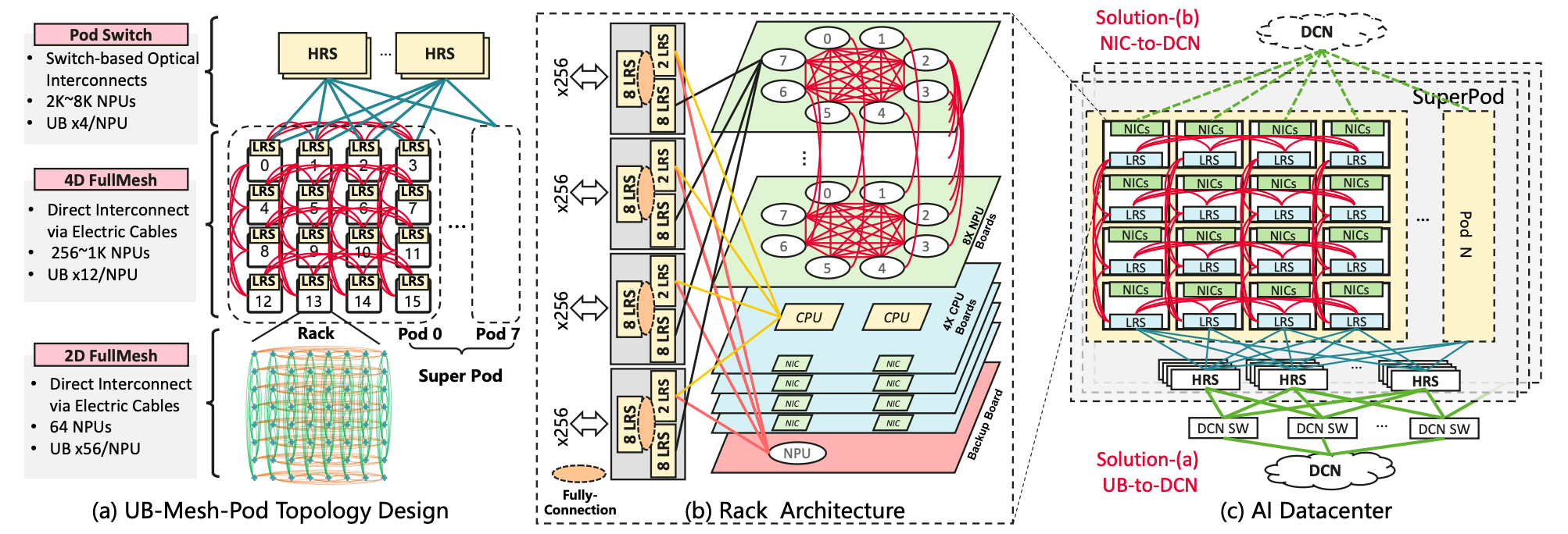
In UB-Mesh for Ascend 950 SuperPoD (nD-FullMesh + CLOS), there are bandwidth cliffs, but it does not matter as it meant for training workloads whose high bandwidth needs are within ground of nodes & NPUs. This approach allows using more copper (direct attach copper, or active copper cable) over optics and requires fewer switches. For large clustered, saving are massive.
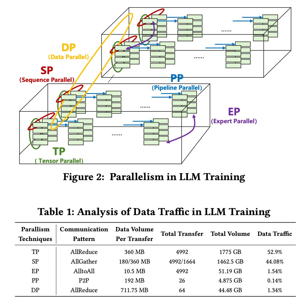
This is how network looks like. The network is organised to maximize use of copper. (red and yellow links), and optics only used to connect pods into SuperPoDs and connect to data center network. Also, lack of switches causes bandwidth cliff, but it is okay due to traffic patterns of LLM training as shown in the above table.
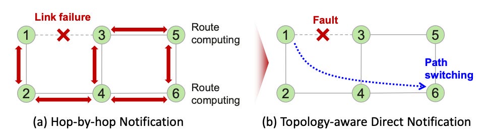
One of the downsides of complex networks like UB-Mesh is that maintenance can be hard. However, the white-paper discusses approaches to deal with them:
The failure-rate problem is answered at the protocol layer and above. UB-Mesh builds reliability into every layer. Link failure are rapidly detected and re-routing is arranged by propagating information/notification about failures.
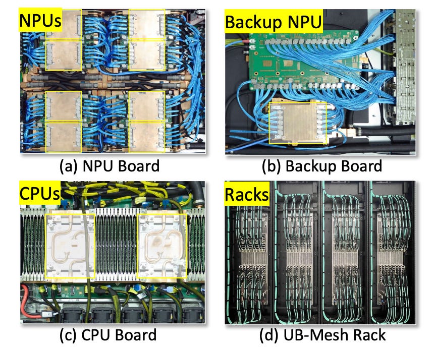
UB-Mesh specifies a 64+1 high-availability design: every rack carries a sixty-fifth NPU as a standby, activated on failure so that an LLM training job continues uninterrupted. Two things about that design deserve notice. First, the granularity: the spare sits on the same fabric, load/store-reachable, so recovery is an allocation decision rather than a topology event - contrast an NVL72, whose seventy-two-GPU coherent island contains no in-domain spare, so one dead GPU degrades the whole domain until a technician arrives (or you stop using the Compute tray; reducing the capacity).
(For this section, we focus on SuperPoD configuration for inference where racks/cabins are organised in rows and NPO is used for communication between NPUs through central cabinets dedicated for switching.)
“For reasons we all know, we don’t have access to advanced process nodes, so we’ve decided to focus our efforts on making breakthroughs by combining chips – essentially connecting more computing resources.” - Eric Xu, Rotating Chairman, Huawei at Huawei Connect 2025
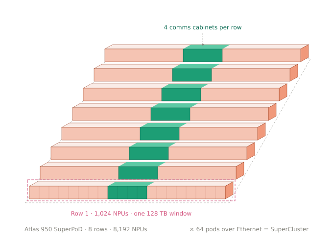
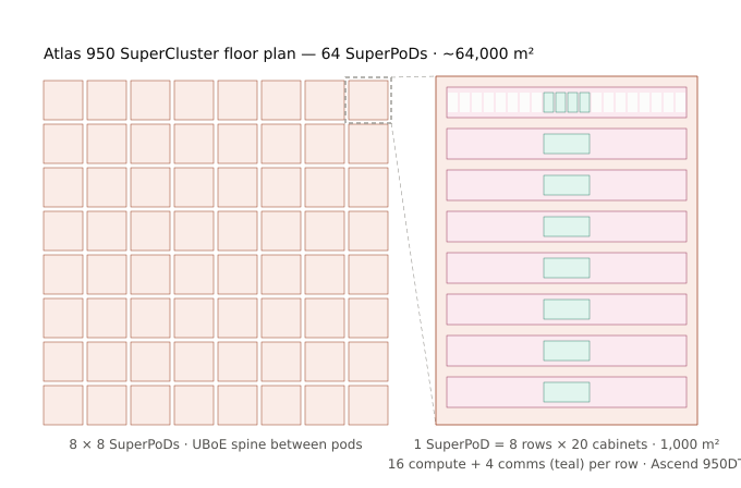
Each 950 SuperPoD consists of 8 rows of 16 NPU cabinets/racks with 64 NPUs in each cabinet/rack, totally 8,192 NPUs (950DT specifically)
There are actually 20 cabinets/racks per row accounting for networking ones, as well. Thus a 950 SuperPoD has 160 racks spanning across whopping 1000 square meters.
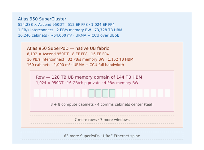
SuperCluster connects 64 such SuperPoDs with 8.192 NPUs each, totalling 524,288 NPUs.
SuperNode Network: UnifiedBus optical interconnect: 16 PB/s and 2,1 μs latency.
SuperNode Performance: 8 ExaFLOPS in FP8 and 16 ExaFLOPS in FP4
SuperCluster Network: SuperNodes can be connected to one another with UBoE in datacenters with existing Ethernet investment
SuperCluster Performance: 524 ExaFLOPS FP8 (for training) and 1 ZettaFLOPS FP4 (for inference).
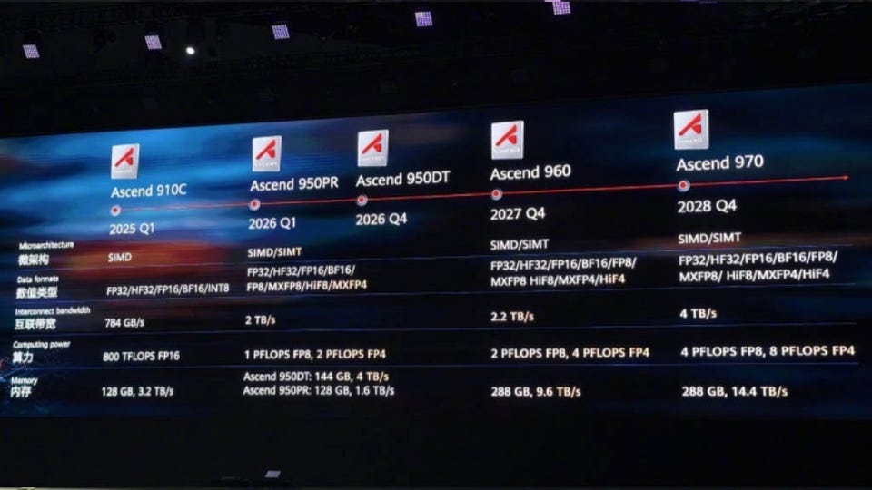
I created this visualisation to help you understand scale of SuperPoD and SuperClusters. SuperPod and SuperClusters to be available from Q4 2026 will use Ascend 950DT chips not Ascend 950PR. They are nearly equivalent chips and differ only in HBM and HBM bandwidth: 144GB at 4TB/s vs 128GB at 1.6TB/s, respectively.
SuperPoD:
SuperCluster:
SuperCluster Data Center:
If you think about it, Huawei has similar philosophy to design datacenters as that of planners of American suburbs: big beautiful home, far apart from one another; far apart from other suburbs and city centers, but connected with wide highways and fast cars.
On the other hand, Nvidia and AMD design for highest possible density of chips in one rack. Their planning reminds you of Hongkong in comparison! Many of their strengths and problems are also rooted in their density.

While SuperPoD blurs distinction between scale up and scale out; let us define scale up on Nvidia terms for sake of comparison. Nvidia defines scale up as domain where GPUs can access each other’s HBM directly. In case of 950 SuperPoD with 8192 NPUs, only 1024 NPUs located in a row can access each other’s memory over UB Memory. So let us take a row as scale up domain for comparison.
16 Ascend 950 cabinets/racks, sixty-four NPUs per rack: 1,024 NPUs, each with 128 GB (for 950 PR) or 144GB (for 950DT) of high-bandwidth on-package memory. Every one of them can read and write every other’s memory synchronously, ordinary loads, stores, and atomics, as if it were local. The row’s total is 128 TB of directly addressable memory. The 950 white-paper caps the UB load/store address space at exactly 128 TB, 2^47 bytes, and 1,024 950PR chips at 128 GB lands on it to the byte. In case of 950DT with 144 GB HBM per NPU, there will be total of 144 TB of HBM across 1024 NPUs. However, going by the white paper, only 128 TB will be directly addressable, additional HBM could be used for other use cases that are local in nature.
The sixteen-rack row is not merely a configuration; it appears to be the design point around which the coherency window was sized. One row equal one flat memory machine (roughly equivalent of NVL72, but with more FLOPs, HBM and memory bandwidth, as we will see soon)
An NVL72 offers roughly 14 TB of NVLink-coherent memory with GB200, about 20 TB with GB300. The Huawei row offers nine times the former. On compute, dense against dense - NVIDIA’s 10 and 15 petaFLOPS of FP4 per GPU for GB200 and GB300 are dense ratings, with sparsity figures double that. Ascend publishes only dense - Ascend 950DT delivers roughly 2 PFLOPs per NPU, totalling approximately 2 exaFLOPs per row (1024 NPUs), against 0.72 exaFLOPs for a GB200 NVL72 rack and about 1.08 exaFLOPs for GB300 NVL72 rack.
Below I present easy to follow comparison between chips and systems.
GPU vs NPU:
Here is comparison of Nvidia Blackwell GPUs and Ascend 950 NPUs in inference topology (FLAT/CLOS). You can notice, while NPUs have significantly more scale out bandwidth, they have lower specifications in other areas.

GPU & NPU Scale Up Domain Comparison
Huawei blurs the distinction between scale up and scale out domain, as we saw. However, direct memory access by one NPU of another NPU is only possible across 1024 nodes (row of 16 cabinets/racks, with 64 NPUs each). Let us use it as unit of comparison with NVL72. NOTE: per Huawei documentation SuperPoDs and SuperClusters are made of Ascend 950DT and not 950PR. Still I present below numbers for scale up domain for 950PR as well, if those NPUs were put in equivalent cabinet & row configuration as for 950DT.

I added this great table for quick comparison. You will notice massive improvements in HBM and FLOPs and very high densities compared to Huawei chips. It will allow you to appreciate ingenuity of Huawei’s design. Despite ‘weaker’ individual components, the system as a whole is arguably more capable.
UB gives software three communication primitives, and the radius of each is different.
UB Memory is the synchronous primitive (1024 NPUs in a row): this one makes the row of 16 racks/cabinets effectively a single machine. A compute core issues an ordinary load, store, or atomic; a decoder resolves which node owns the address; the operation crosses the fabric; and the peer chip’s memory-management unit translates and permission-checks it before touching memory directly. No queues, no software, no driver in the path - remote memory is simply memory (this is how NVLink domain behaves). Its span is the 128 TB address window on the 1,024-NPU row.
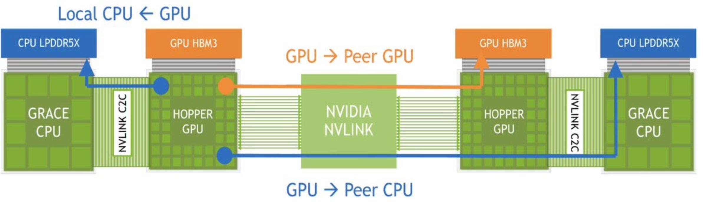
In Nvidia ecosystem, this idea is around for long. NVLink allows one GPU to access another GPU’s memory if they are connected with NVLink. Beauty of NVL72 (that is available from Blackwell generation) is that 72 GPUs of the rack can access each other’s memory. For Blackwell generation, they can do it at 900 GB/s per GPU (unidirectional) and for Rubin generation, they will be able to do it at 1800 GB/s per GPU (unidirectional). This allows NVL72 to host very large models effectively. But this scales only to 72 GPUs. Beyond 72 you have to use much slower scale out network and direct memory access is not possible. Please also note GPUs inside NVL72 domain can also access CPU LPDDR memory, called as host memory. Below is a diagram for Hopper to show such connectivity (for Blackwell/Rubin I did not get an equally nice diagram, but they also have similar direct access with their NVL domain).
URMA is the asynchronous primitive: A compute core (or the hardware scheduler itself) rings a doorbell on a Jetty queue; dedicated hardware executes the transfer - writes, reads, sends, fetch-add and compare-and-swap atomics - and posts a completion, while the core goes on computing. It runs over two transports: a reliable mode with end-to-end retransmission sustaining four ports of bandwidth, and a lightweight mode that trusts the fabric’s link-layer reliability and sustains nine - a full terabyte per second each way. URMA’s span is everything: the whole 8,192-NPU SuperPoD over native UB, and even past it over UBoE (UB over Ethernet). Recall 64 8,192-NPU SuperPoDs can be connected into a SuperCluster with close to half a million chips in total!
URMA is equivalent of GPUDirect RDMA of Nvidia world (diagram below), but at much higher bandwidth of 1008 GB/s unidirectional (if the network if FLAT/CLOS) compared to 50 GB/s for GB200 and 100 GB/s for GB300 scale out network.
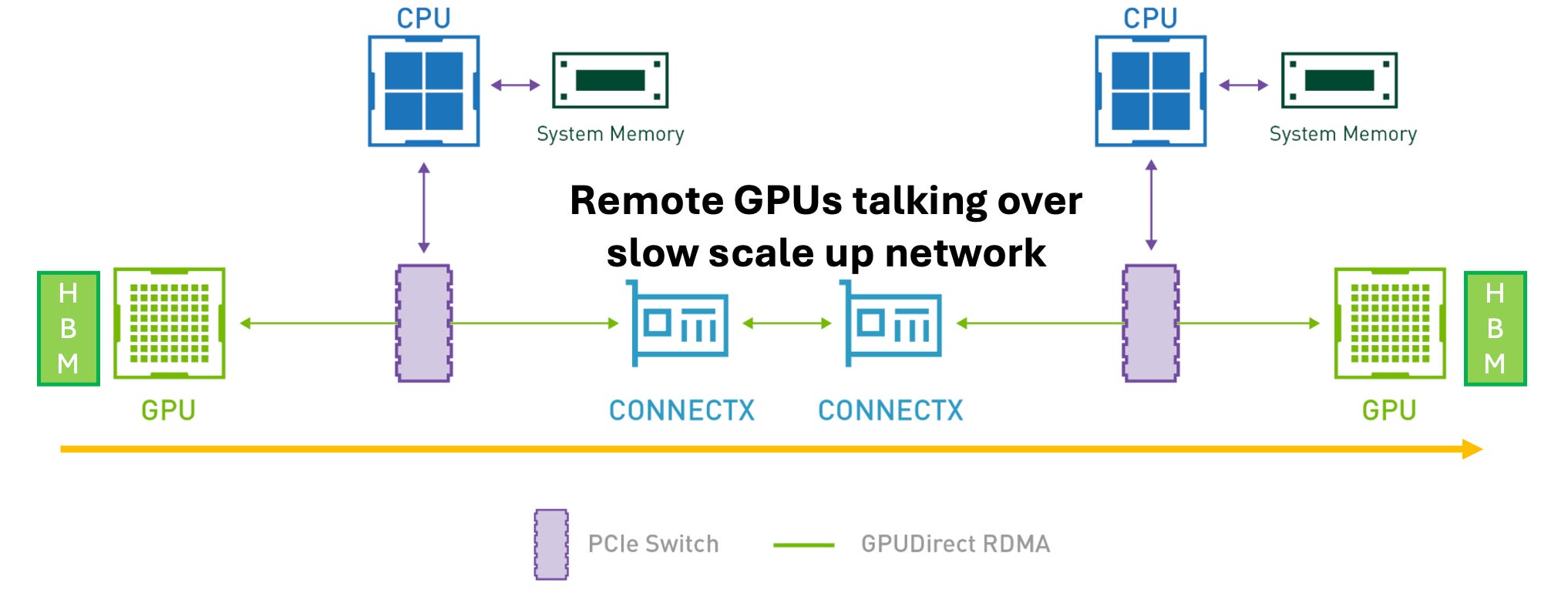
The CCU is the collective primitive - this is equivalent of NCCL in Nvidia world and has hardware implementation. The Collective Communication Unit (CCU) receives whole collectives (AllReduce, ReduceScatter, AllGather, All2All and kin) from the on-chip scheduler, unrolls them into fine-grained parallel steps, and executes each step as one of exactly two things: a Reduce, computed in the CCU’s own Reduce Units against its own MemorySlice storage, or a URMA transfer. Read the block diagram closely: the CCU exposes precisely two call interfaces - Reduce and URMA (asynchronous that can reach entire SuperCluster). There is no UB Memory (synchronous) path. The collective engine does not use synchronous communication at all.
By building collectives exclusively on URMA, the CCU inherits URMA’s span which is much larger than that of UB Memory’s: it spans all eight rows of the SuperPoD (8192 NPUs), and because URMA rides UBoE extends in principle to any NPU reachable over Ethernet (entire SuperCluster in theory). CCU also inherits URMA’s bandwidth and in a FLAT/CLOS networks it is massive. Contrast the Nvidia’s software equivalent: NCCL must change transports at the NVLink boundary, switching from peer memory access to network verbs, with hierarchical tricks to hide the boundary crossing. The CCU uses one mechanism for the entire span, so a collective algorithm has the same shape at 64 chips and at 8,192 and beyond. Interestingly, movement and reduction both happen in dedicated silicon, off the AI cores and largely off the system bus.
For readers fluent in the NVIDIA stack, the mapping is worth making explicit - because it is diagonal, not one-to-one:
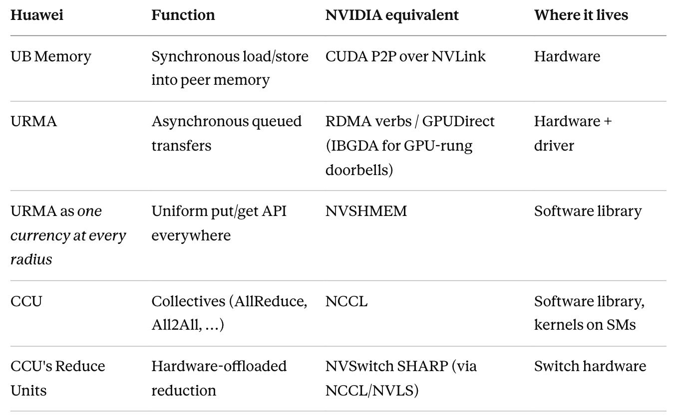
NVSHMEM’s job is presenting one put/get/atomic API that quietly uses NVLink load/store inside the NVLink domain (72 GPUs) and GPUDirect RDMA outside it. It is a software library that uses two mechanism/protocols. NVSHMEM hides difference in scale up and scale out networks from the software using it. In Huawei world, the network mechanism is URMA across all the NPUs for equivalent communication, so it simplifies the design of NVSHMEM type libraries.
NCCL, meanwhile, matches the CCU’s function: both execute collectives, but NCCL is kernels running on the GPU’s own compute units - paying the tax in SM cycles, and switching transports mid-algorithm at the NVLink boundary. NVIDIA’s true hardware collective offload, SHARP, sits in yet a third place: the switch. NCCL’s equivalent in Huawei world is CCU. It has silicon for compute in form of Reduce units and it uses URMA mechanism to talk to all the NPUs.
The world’s most datacenters run on Ethernet and a new fabric that cannot interoperate with Ethernet will have challenges in adoption. The Ascend 950 white-paper offers two integration paths.
Option 1: Conversion in the switch. In this approach, the SuperPoD’s interior stays pure UB - every chip keeps its full eighteen-port pool on the native fabric - and the UB Switch itself performs the UB-to-Ethernet conversion at the boundary, presenting standard Ethernet uplinks to the datacenter spine. The whitepaper’s framing is that the SuperPoD joins existing Ethernet networks seamlessly at no extra hardware cost, because the conversion happens in switch silicon the SuperPoD needed anyway.
Option 2: Conversion on the chip itself. The Ascend 950 chip can also join Ethernet networks directly via UBoE technology, networking over industry- standard Ethernet switches. Each Ascend 950 can dedicate two of its ports to UBoE - 2×400 Gbps of the UB protocol carried directly over industry-standard Ethernet switches.
The interior mesh remains native UB (the diagram is explicit: the chips stay green-wired to each other).
Note, NVIDIA offers no equivalent: NVLink never converts to Ethernet in a switch or on the GPU itself. You need discrete NICs for scale out with Ethernet. Scale up (NVLink) and Scale out (Ethernet/Infiniband) are totally isolated from one another with no port sharing.
If is fair question. Writing white papers like Tau Scaling Law is easy, but will these approaches work in production? Let us tackle objections one by one (we continue to focus on Ascend 950 SuperPoD with FLAT/CLOS network):
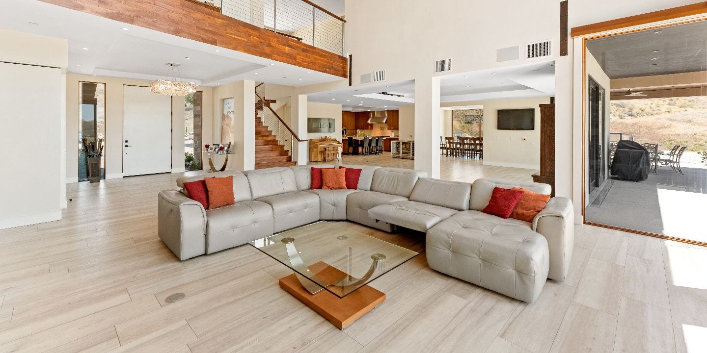
Sixteen racks/cabinet in row of Ascend 950 SuperPod against one NVL72 is unflattering, to be clear! But the objection has cause and effect backwards. NVIDIA’s situation is not a virtue; it is a symptom - the result of copper’s two-meter max length and Nvidia’s approach of using NICs/Ethernet for scale - out. Since scale-out network is slow, so Nvidia’s focus is on compute and memory density within NVL72 domain. Huawei’s 1,024 NPUs spread across a full row precisely because their special design of network permits it. The sprawl actually makes thermal design also easier.
It will take a lot of space, but so what? Density was never the goal; it was the constraint. If you are rich, you build a big house and live comfortably. You do not cram into a studio and call it discipline.
Ascend 950PR’s memory bandwidth at only 1.6 TB/s, and that of 950DT’s at 4 TB/s trails 8 TB/s of NVIDIA’s current HBM3e HBM in Blackwell generation (Rubin generation uses HBM4 reported to have bandwidth around 22 TB/s). Per chip basis, Huawei is behind on the memory bandwidth and will remain behind for considerable future… Are they doomed then?
No, per-chip bandwidth is the wrong consideration for the workloads that is the most common: Mixture of Expert (MoE)! In MoE models - an architecture where China based labs excel - some ninety percent of parameters are in Mixture of Expert (MoE) layers, and expert parallelism (EP) spreads those experts across as many devices. Each token in a given batch accesses only a few experts in each layer; so what governs aggregate decode throughput is total memory and total memory bandwidth across the pool of devices.
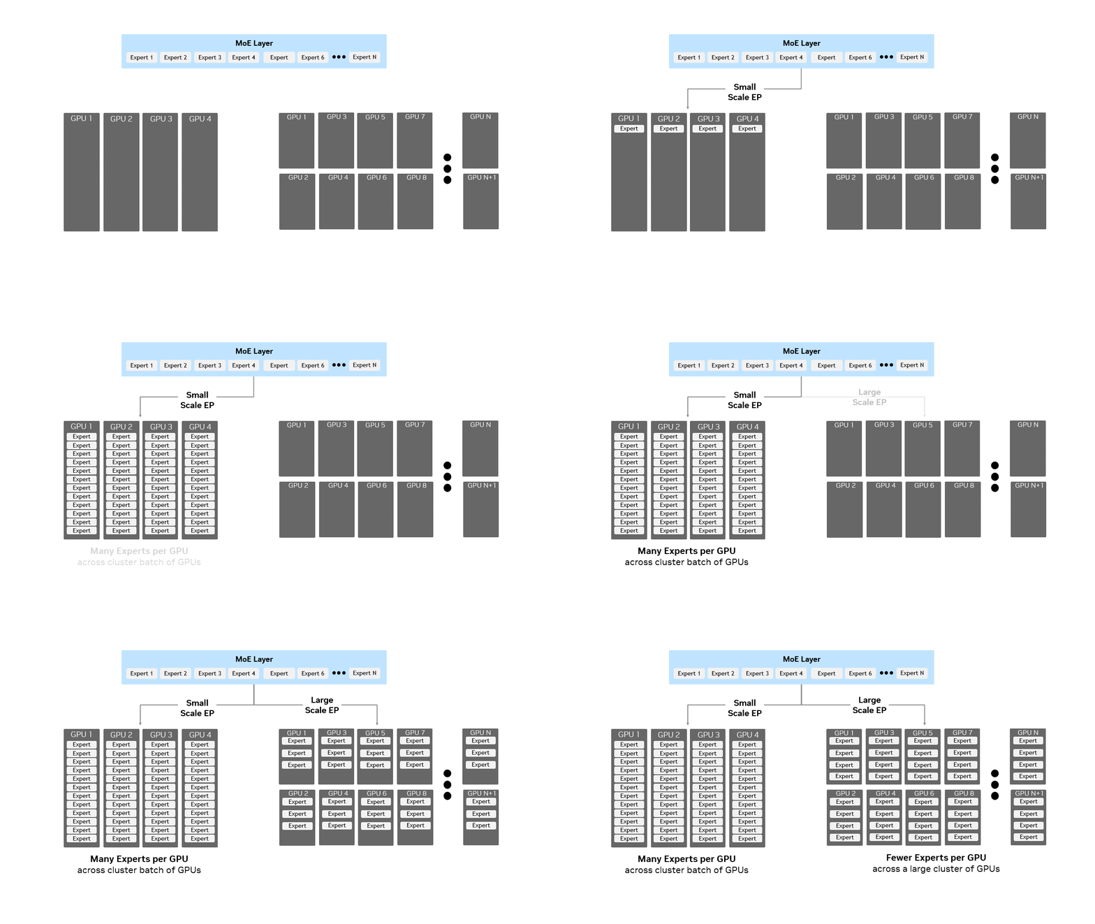
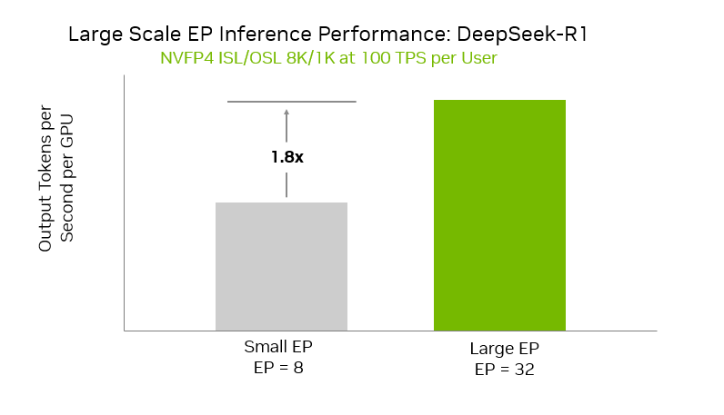
Wider you are able to spread your expert (WideEP), fewer experts each GPU/NPU needs to support. This results in higher overall throughput for token generation. For example EP=32 results in 80% higher throughput per GPU compared to EP=8. This is how you can work with GPUs/NPUs with lower HBM bandwidth.
Ascend 950 SuperPoD’s single row (16 racks with 64 NPUs each) that has 1024 NPUs that have 4,096 TB/s of aggregate bandwidth compared 576 TB/s for NVL72.
It has 144 TB of capacity (of which 128TB can be on UB Memory address space) against 14 TB of GB200 NVL72 and 20TB of GB300 (approximately). Huawei offers bigger domain across which experts can be spread, its total HBM and HBM Bandwidth is many times higher than NVL72 system. So they can host really large models like even Kimi 3 with nearly 3 trillion parameters.
Many chips works in parallel as a single chip is why Huawei could afford to regress on FLOPS even against its own 910C (at FP16). The philosophy is that the system-level performance, not the per-chip one, decides how well you can serve trillion-parameter models economically.
Ascend 950 racks/cabinets are connected with NPO (Near Packaged Optics). In a FLAT/CLOS topology all the NPUs are connected to switches at center with NPO, that is why any NPU to any NPU latency is uniform.
UB-memory access (equivalent of NVLink) works across entire row of 16 racks/cabinets i.e. 1024 NPUs. Moreover all 8,192 NPUs of a SuperPod can communicate with one another at UB bandwidth with URMA in FLAT/CLOS topology.
The article quotes hops around 2.1 microseconds against NVLink’s sub-microsecond copper. However, as you would recall NVLink connects only 72 GPUs, beyond it you would use NIC + Ethernet/Infiniband, it would have much higher overall latency. So Huawei’s approach offers to connect up to 1024 NPUs with UB Memory (NVLink equivalent) and all 8,192 NPUs in a SuperPod with URMA (RDMA equivalent) at full UB bandwidth and uniform 2.1 microseconds latency. It is a pretty good latency for such large group of NPUs (note: latest Huawei material quotes 3 microseconds).
To put in another way, NVIDIA’s latency profile is not “fast”; it is bimodal - magnificent inside a small circle (NVL72 rack), worse than UB outside it. Huawei’s is flat: 2.1 microseconds to any of a thousand peers of a row (even to 8192 peers within a SuperPoD), no cliff! For any model too large to live inside seventy-two GPUs, which is to say, all the future models on path to AGI & ASI, Huawei’s uniform microseconds latency beats bimodal latency profile.
(A careful reader will now be holding two latency figures in apparent tension: the roughly 100 nanoseconds of remote access claimed by the τ-scaling paper, and the 2.1 microseconds quoted here from Huawei Connect 2025 event. My read is they measure different segments of the same journey.
The ~100 ns is the protocol’s toll - the cost of issuing and completing a memory-semantic operation through UB hardware, the segment that TCP/IP-class software stacks inflate to tens of microseconds and the segment to which the paper’s ~500× compression refers.
The 2.1 µs is likely the whole trip: SerDes, electro-optical conversion, fiber, and switch hops between cabinets. Light travels at nearly 200k km per second in fibre optics, so it takes about 1 µs to travel 200m; add switch traversals and the 2.1 µs budget is nearly accounted for.)
And the microseconds of UB protocol themselves are largely hidden by design. The Ascend 950 chips are built to keep cores blind to fabric latency: asynchronous URMA transfers overlap with compute, the CCU runs collectives without occupying a single AI core, and hardware scheduling dispatches at nanosecond granularity.
A thousand NPU packages offer for two and a half times the dense FLOPS (compared to GB200 NVL72). Surely the performance-per-watt based comparison makes Huawei look ridiculous, right?
Not necessarily. For Huawei’s actual customers, the binding constraint is not watts; it is access to silicon at all. Against that constraint, the design is ruthlessly rational. Mature DUV nodes with multi-die packaging yield far better than reticle-limited monoliths on bleeding-edge processes. The memory is Huawei’s own HiBL & HiZQ rather than scarce, sanction-priced HBM from two Korean suppliers. The optics are linear-drive, deleting the DSP that burns a large share of a pluggable module’s power. Also, the sprawl (large number of racks) that looked wasteful in Objection One offers a thermal dividend: heat spread across a row is cheaper to remove than heat crammed into copper’s two-meter radius domain (recall all the trouble Nvidia is having with Rubin Ultra and Kyber racks due to high density). And the whole stack - chips, optics, switches, racks - is vertically integrated, with no seventy-five-percent gross margin stacked on top by Nvidia. China is growing electricity production at historic rates. Huawei is spending the abundant resource (power, floor space, mature fab capacity) to deal with not being able to manufacture most advanced nodes that Nvidia has access to. That is a a smart trade off, I would say, and every generation of the Tau curve - e.g. the 950DT’s doubled memory bandwidth compared to 950 PR being the first instalment - reduces the per-package gap while the systems advantage compounds.
CANN (Huawei’s equivalent of CUDA) ecosystem must achieve what CUDA ecosystem has achieved over a much longer period. CUDA ecosystem is both older and larger. But even here the trajectory favours the challenger - the stack is open-source, developers must manage just one fabric instead of three, and the hardest orchestration problems (collectives, scheduling, data movement) have been pushed into hardware precisely, so software developers have less to worry about.
Optics is not a miracle medicine. Optical links fail more than copper - and no one says so more bluntly than Huawei’s own engineers, whose UB-Mesh presentation at Hot Chips 2025 put optical error rates two to three orders of magnitude above copper’s, and treated node failure at SuperPoD scale as a matter of when, not if. Conventional optical modules (trans-receivers) are power gluttons: a DSP-based 800G pluggable draws 14 to 17 watts.
All true. But Huawei is not deploying “optics” in the abstract; it is deploying one deliberately chosen point in the optics design space, with everything co-designed/co-engineered by them - and each of the three failure modes above is attacked by a specific choice.
The power and conversion-latency problems fall to linear-drive optics. The τ-scaling paper describes Hi-ONE, the High-density Optical-interconnect-Node Engine: a Near-Packaged Optical (NPO) engine delivering 8 Tb/s per module, enough to carry an entire AI chip’s UB bandwidth on a single optical link. Its signal path is exactly the linear architecture we commonly call LPO, though the paper never uses the term: an analog equalisation driver and trans-impedance amplifier in place of a DSP. Industry measurements of this approach show a 40 to 50 percent cut in module power - down to 7 to 8.5 watts at 800G - and per-hop latency under 3 nanoseconds, versus 8 to 10 for DSP modules. What makes DSP-deletion safer is a trick: the UB protocol deliberately tolerates a relaxed bit-error rate, letting the transport layer absorb the errors the physics layer causes - a cross-layer trade between protocol and photonics that is only available to a designer who owns both. That is the catch that has stalled LPO in the merchant market - it demands exquisite SerDes linearity and tight co-engineering of module, ASIC, channel, and protocol that multi-vendor ecosystems struggle to coordinate - and it is precisely Huawei’s moat. As designer of the HiLink SerDes, the optical engine, the switch silicon, and the protocol, it is one of the few companies on earth that can close the linear-optics loop by fiat rather than by committee.
Hi-ONE’s near-package placement cuts the required electrical SerDes reach from roughly 100 centi-meters to about 5 - collapsing the lossy copper run that DSPs existed to compensate - while extending link reach from under a couple meter max to 100s of meters, which is what renders a gigawatt-scale, datacenter physically buildable at all. Interestingly they do not choose Co-packaged Optics (CPO), as it is complex to manufacture even though it saves a little bit more power. NPO is the pragmatist’s point on the curve: most of CPO’s electrical benefit, at pluggable-class manufacturability and cost.
One objection remains, and it follows arithmetically from everything above: if Huawei needs more chips per FLOP, it inherits more failures per FLOP. Match a full SuperPoD’s 16.4 dense exaFLOPS with GB200s and NVIDIA needs about 1,640 GPUs to Huawei’s 8,192.
Per Epoch AI, for example, a single H100 SXM GPU fails approximately once per 50,000 hours,1 but this rate scales linearly with hardware count. Consequently, a system with 16,384 GPUs experiences a failure every 3 hours on average, while a larger system with 1 million GPUs faces a failure every 3 minutes.2”
Huawei has nearly 5 times more NPUs for the same flops (2 PF FP4 for Ascend 950 NPU vs 10 PF FP4 for GB200 GPU), so failures are higher in absolute count and so are cluster interruption.Add unproven silicon, proprietary memory, and a hall full of optics and picture starts getting even more complicated: the fleet seems too large just to keep alive long enough to train anything. Astute readers will remember “Square Cube Law” at this point.

Epoch AI, analysing exactly this question for NVIDIA-class clusters, showed that failure overhead does not scale with cluster size - it scales with its square root. The optimal checkpointing (weights, optimiser states) cadence balances checkpoint cost against expected loss, and at that optimum the fraction of training time lost grows as the root of (checkpoint cost × chip count × failure rate). Five times the chips costs roughly 2.2 times the overhead, not five; two and a half times costs about 1.6. And the level of that overhead is set almost entirely by one variable: how long a checkpoint takes. Write checkpoints to storage (like AWS S3) and the overhead sits near a couple of percent; write them into the spare memory of peer accelerators, a few replicas each, and recover by reading them straight back from those peers over higher speed network, and the checkpoint cost collapses to sub-second. Run the numbers at 8,192 chips, a chip failing every six hours with peer-memory checkpointing and the training time lost lands under half a percent. Epoch’s conclusion for NVIDIA - hardware failures will not limit scaling - applies to Huawei chips as well, as they do not assume any specific characteristic of Nvidia chips in their analysis.
Interestingly, nearly every mitigation Epoch prescribes as a technique on NVIDIA hardware exists as a primitive on this architecture.
Peer-memory checkpointing presumes spare memory - the 950DR carries roughly 72 GB per dense petaFLOP against NVIDIA’s 19 GB per dense petaFLOP (recall GB200 has 192GB HBRAM and 10 petaFLOPs for FLP4), pretty good room for replicas beside the optimiser state!
It presumes fast paths to peers - the fungible terabyte-per-second pool, with SDMA engines moving checkpoint bytes while the AI cores keep training. It presumes recovery can read a dead node’s state from its peers - which, inside the 128 TB window, is not an RDMA choreography at lower bandwidth, but a load instruction more like NVLink access at high bandwidth. This allows the replacement NPU to gain access to predecessor’s replicated state faster.
It presumes spares that can rejoin quickly - and as described in response to Objection Five: the sixty-fifth NPU standing by in every rack, on the same fabric, activation being an allocation decision rather than a repair event, where an NVL72 contains no in-rack spare at all. And beneath the checkpoint layer entirely, the memory’s own RAS machinery - online ECC, patrol scrubbing, transparent row-sparing - absorbs a whole class of faults before they ever register as a failure.
In a post-Moore world, one can say, the fabric is the computer. NVIDIA built the world’s best small circle (NVL72, and NVL144 for Kyber racks) and must now fight physics to widen it; Huawei, barred from the transistor desnity race, built a world without a circle at all - and aimed it squarely at the place the Nvidia’s architecture is weakest: the boundary where copper ends (scale up) and optics begins (scale out). Huawei has simply decided there shouldn’t be a distinction between scale up and scale out network capabilities/bandwidth: they design their topology, chips, connecters and switches for that. They will have lot of friction initially, but once they cross to the other side they would have achieved the escape velocity!
It is long known that clouds and enterprises in China use Huawei clusters for inferencing. Now we also have evidence that 1.6T parameters models are being trained on Huawei cluster.
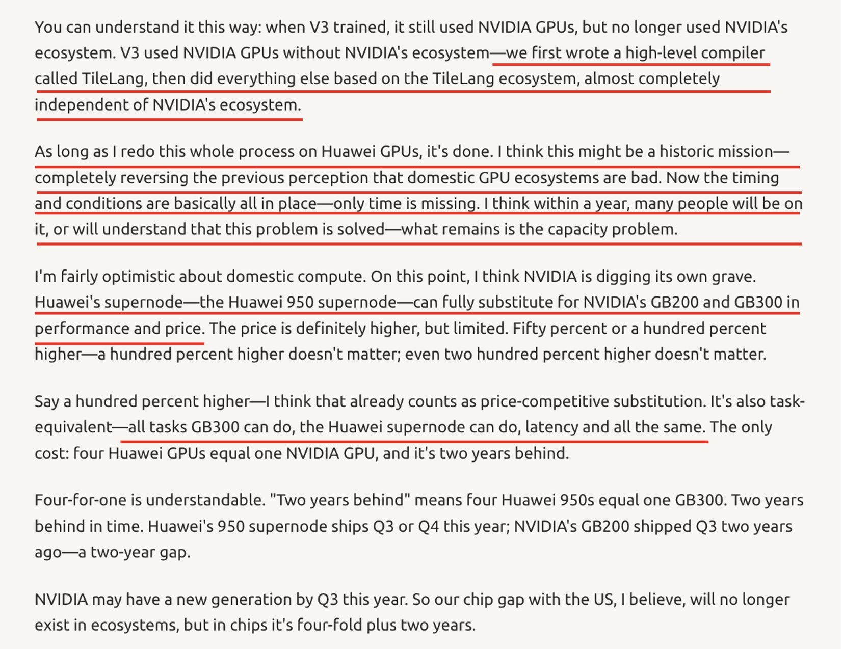
DeepSeek CEO Liang Wenfeng gives Huawei’s strategy a vote of confidence, in his leaked conversation with his investors.
Epoch AI’s Hardware failures won’t limit AI Scaling essay.
UB-Mesh paper (64+1 high-availability design; direct-notification link-failure recovery) and Hot Chips 2025 presentation
Eric Xu keynote, Huawei Connect 2025 (UnifiedBus reliability and fault-switching claims)
SemiAnalysis for comparison of Nvidia GPU
τ Scaling Law paper, v2 (adds UnifiedBus, Hi-ONE, and 3D Folding; network-scale τ analysis)
Positive impact of design of UB extends to many other areas such as KV caching. Also Ascend 950 design includes CPU cores. This bonus material talks about that.
Agentic AI is a memory problem due to long context that long agentic trajectories need. Ultra-long contexts, multi-turn sessions, long-horizon plans - every token a model has attended to or generated leaves a key-value residue that must be kept warm for the next turn, and the whitepaper understands that this demand is growing exponentially, beyond what any accelerator’s on-package memory can hold. HBM is the most expensive real estate in the datacenter (have you seen memory stocks lately?); saving a dormant chat session’s cache there is like renting a Manhattan apartment to store winter clothes…
The conventional remedy is offload: spill KV blocks to the host CPU’s DRAM over PCIe and pull them back on resume (and to SSD if it is not going to be used soon enough). On standard systems that path is narrow and crowded - 64 GB/s per direction of PCIe 5.0, shared with everything else, with the host CPU’s software stack managing every transfer. NVIDIA’s answer connect CPUs and GPUs with ultra fast NVLink CC. For example, GraceBlackwell superchip, connects a CPU and its half-terabyte LPDDR to each of the two GPU over a 900 GB/s NVLink CC link. This is great. Also, GPUs can access other CPU’s LPDDR as well, as long as, they are on the same NVLink domain. But NVLink domain is only 72 GPUs!
Huawei’s answer is the ultra-large CPU memory pools over UB. Racks of CPUs fronting memory pools attach to the UB fabric as first-class citizens, and - per the white-paper - the compute chips of a rack/cabinet access that pool directly through their UB ports, at high bandwidth and low latency, making full use of CPU memory resources (more details on it are not available though).
If you look closely at the chip’s floor plan and something unusual can be seen. Inside each AI die - not beside the package, not across a PCIe slot, but embedded at the corners of the AI Core array itself - sit general-purpose Linx816 CPU blocks, sharing the die with the compute they serve. The full chip carries four clusters of two cores each: eight ARMv8-A cores, sixteen hardware threads (the spec sheet’s “8C16T” bin is exactly this), each cluster with its own L3, all of it hardware-cache-coherent with the AI cores’ L2 and the shared on-package memory. The NPU has a CPU living inside it!!! This is quite unlike any design by Nvidia, AMD or Amazon.
Why plant CPUs in an NPU’s ? Because the control plane has a τ problem too. In the conventional Host–Device arrangement, every piece of housekeeping - page-table maintenance, operator compilation, performance monitoring, the scheduling of accelerators and IO - lives on the host, tens of microseconds away across PCIe and a driver stack. As kernels shrink toward the microsecond scale, that round-trip starts being significant. Huawei’s answer parallels its data-plane answer: collapse the distance. The embedded AI CPU runs an operating system on the device, absorbing the housekeeping locally; awkward operators that fit neither Cube nor Vector - control-heavy logic, general scalar work - execute in place instead of bouncing to the host - this saves lot of time! Interestingly, the CPU blocks sit adjacent to the L2 slices of the core arrays they manage (more on it in one of future essays)
The latest Tau scaling law paper is very eloquent on this. So providing its explanation, as it is. Highly recommended to read it