PCB Tracer Software for Reverse Engineering, Troubleshooting & Repair Now with KiCad support
Launch PCB Tracer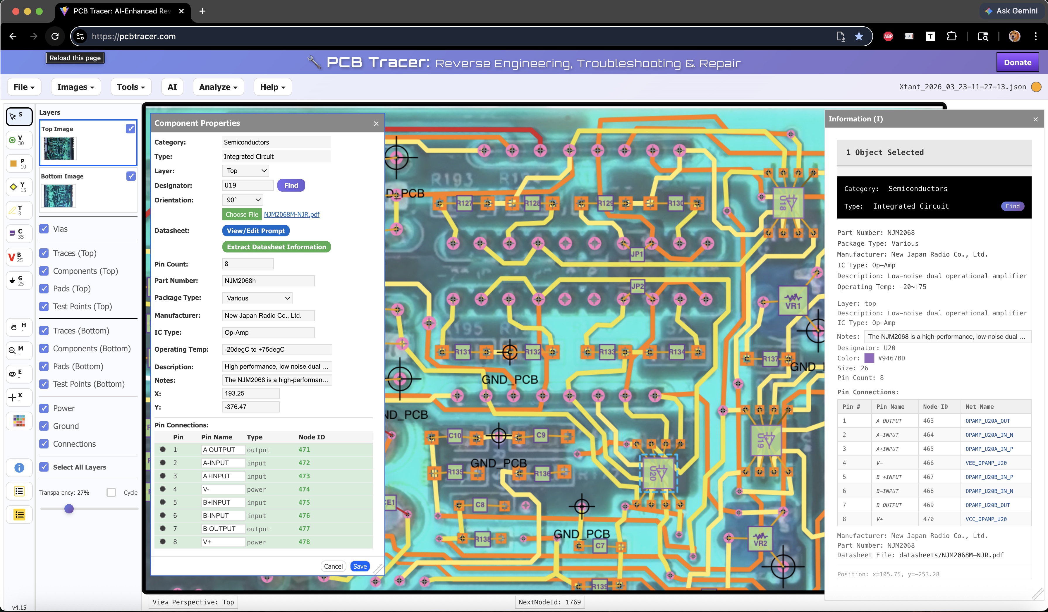
The PCB Tracer workspace with menus, tools, layer controls, and component connectivity
Tracing connections through vias on a multi-layer PCB is difficult, tedious and error-prone — especially when there are no schematics available. Whether you're repairing vintage gear, analyzing an unknown board, or documenting a design, you need a way to follow signals across layers accurately.
PCB Tracer is a free browser-based tool for reverse engineering PCBs. Load photos of your board's top and bottom, overlay them with adjustable transparency, and annotate every trace, via, pad, and component. The tool tracks connectivity through unique node IDs, building a structured, data-rich model of your circuit — not just a drawing.
Benefits
Because PCB Tracer builds a structured model — with typed components, IC properties, named pins, and tracked connections — you get capabilities not possible with a drawing tool: generate netlists with logical net names, export KiCad schematics, predict expected measurements, troubleshoot with AI assistance, and get plain-language circuit explanations that help you truly understand your board.
Signal Path Visualization
Adjustable transparency lets you see top and bottom layers simultaneously, so you can follow a signal from a top-side trace, through a via, to the bottom layer and back. Hover over any component or pin to see designator, value, pin names, connections, and net membership.
Schematic Generation (beta)
Generate schematics directly from your traced components, connections, and netlists. Export to KiCad format for further editing in KiCad's schematic editor.
Logical Net Names
AI analyzes your components and connections to generate meaningful net names automatically — VCC_3V3, SPI_CLK, AUDIO_OUT instead of N$1, N$2, N$3.
Circuit Analysis
AI-powered analysis tools for understanding and diagnosing the circuit:
- Circuit Explanations — generate a technical report covering power distribution, functional blocks, and signal flow
- Troubleshooting (beta) — using the problem symptoms and test point measurements you provide, AI examines components, connections, and netlist to suggest failure points, test sequences, and root causes
- Expected DMM Readings — select any two electrical nodes and compute the expected resistance, capacitance, and impedance between them using Modified Nodal Analysis, then compare predicted values with actual probe readings to pinpoint damaged traces, cold solder joints, or degraded components
Bill of Materials Export
Export a complete BOM in JSON or PDF format. Includes designators, values, manufacturers, part numbers, and package types for every documented component.
AI Component Identification
Enter component markings, a photograph, and contextual information, and AI cross-references manufacturer databases to identify the part, extract key specifications, and populate properties — with confidence ratings on the results.
No Installation Required
Runs locally in the browser. No installation, no OS restrictions.
How PCB Tracer Works
PCB Tracer: turn photos into a connected network of data-rich components
- Photograph your PCB — top and bottom surfaces, with good lighting
- Load both images into the browser-based tool
- Overlay with transparency — a "virtual X-ray" with automated slider lets you see through layers
- Align and transform — use scale, nudge, rotate and other tools to quickly align images
- Annotate everything — draw traces, place pads/vias, add components with properties, designators and connections managed via unique nodeIDs
- Create IC objects from datasheets — upload a PDF datasheet and AI extracts key component properties to convert the generic IC from PCB Tracer's component library to any specific IC
- Generate netlists — AI analyzes components and connections to generate netlists with logical net names
- Export KiCad Schematics (beta) — generate KiCad-compatible schematic files from your annotated PCB data
- Analyze your circuit — analysis features support probing comparisons, circuit troubleshooting, and more
Key Features
Virtual PCB X-Ray and Perspective View Controls
Use the automated transparency slider to visualize both layers simultaneously. Toggle between Top and Bottom views or change the perspective view with simple controls.
17 Tools and 14 Layers for Organized Annotation
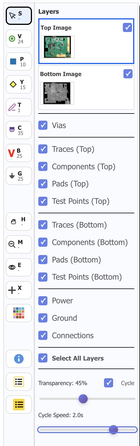
The left-side toolbar provides 17 dedicated tools for every annotation task — selection, drawing vias, pads, and traces, placing components, defining buses and test points, finding components and nets, measuring, erasing, capturing notes, and changing colors.
The layer system gives you fine-grained control over what you see and edit:
- Top/Bottom Images — photos of each side of the PCB
- Vias — connection nodes linking PCB layers
- Pads (Top/Bottom) — component pads on each layer
- Traces (Top/Bottom) — traces on each layer
- Components (Top/Bottom) — data-rich objects with designators
- Power Buses — support for multiple independent voltage buses
- Ground Buses — support for multiple independent ground buses
- Test Points — objects to hold measurement data, notes, etc.
Each layer has visibility controls, so you can focus on exactly what to work on.
Object-Oriented, Data-Rich Component Management
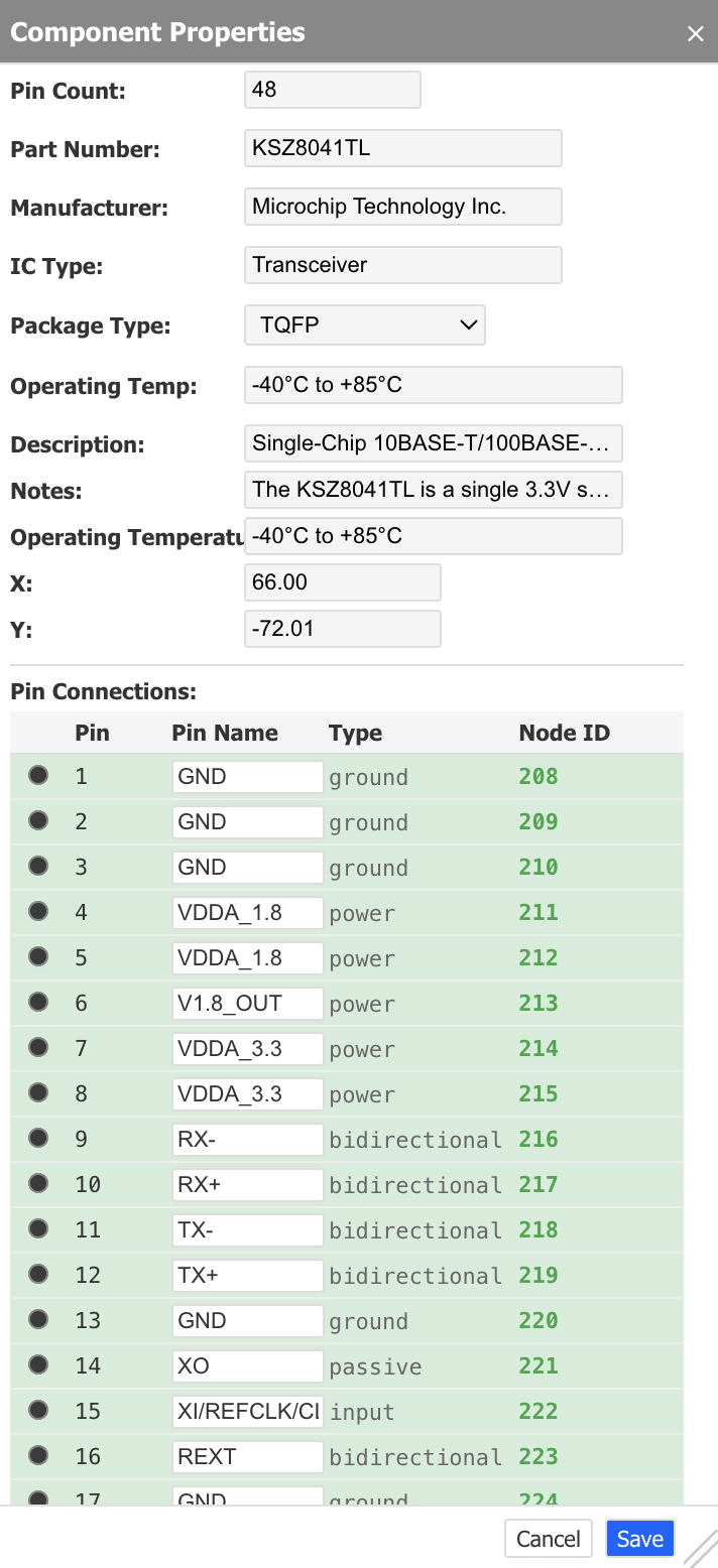
Every component carries context-specific properties:
- Library of common components — 60 electronic components plus AI generation of any integrated circuit
- Component-specific properties — context-specific, configurable properties for every component
- Rollover information — hover over objects for popups showing contextual data
- Pin definitions with names — not just dots, but properly defined connection points
- Unique node IDs — every pad, via, and pin gets a persistent identifier
- A Notes field on each object instance allows flexible data capture
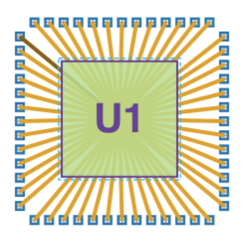
- Automatic designator generation (U1, R1, C1...)
Annotations are structured data, not pixels — enabling connectivity analysis, netlist generation, and AI-assisted diagnostics.
NodeID-Based Connections
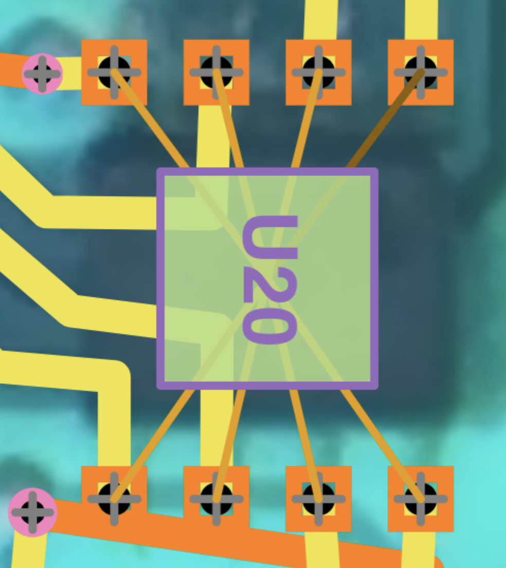
Every connection point (vias, pads, component pins, power, ground, test points) has a unique NodeID. Traces snap to vias and pads, and the system tracks exactly which nodes connect to which — enabling network analysis not possible with drawing applications.
Hover your pointer over any via, pad or component and get context-specific information that includes pin number, pin name, net name, and component properties.
AI-Powered IC Object Creation
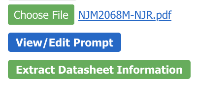
Start with the generic IC from the component library. Then feed PCB Tracer a PDF datasheet:
- AI extracts the IC type, description, pin names, pin numbers, pin types, package info, and more
- Creates a complete, accurate IC object with all properties and pin definitions
- Works with any integrated circuit datasheet
AI Assisted Component Identification
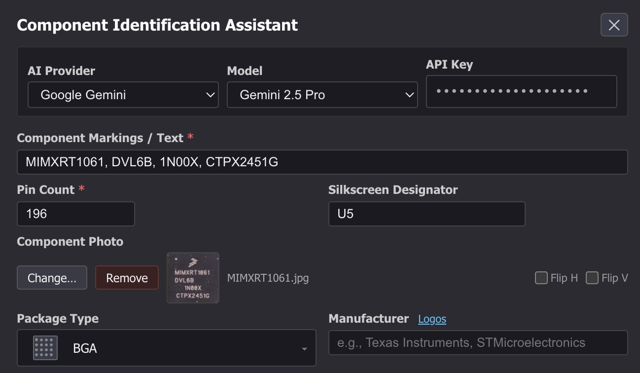
Having trouble identifying a component? The Component Identification Assistant helps you identify it:
- Provide available information — markings, pin count, package type, dimensions, and an optional photo
- AI analyzes the inputs and cross-references known components to produce confidence-rated identification candidates
- A second AI verification pass reviews the results before presenting them, improving reliability
- Results are delivered as a downloadable PDF report including availability status and purchase links
- A built-in reference page of 451 semiconductor manufacturer logos helps decode manufacturer markings
AI-Generated Netlist with Logical Net Names
Once you've annotated your PCB, the AI-based netlist feature can analyze the complete picture:
- Examines all components, their properties, and pin names
- Traces connections through the NodeID-based connection graph
- Generates a netlist with intelligent net naming (not just N$1, N$2...)
- Names like "VCC_5V", "CLOCK_IN", "MOTOR_DRIVE" based on connected component pins

Hybrid Net-Centric Netlist Format
PCB Tracer exports a JSON circuit description optimized for both human investigation and AI-assisted analysis. The format combines net-centric organization with component-centric detail:
- Bidirectional navigation — trace signals from net-to-components or component-to-nets
- AI-ready structure — enables pattern matching, anomaly detection, and signal flow analysis
- Signal, power and ground paths — preserved for intelligent fault detection
- Comparison-ready — compare traced boards against reference designs or parallel circuits

A reconstructed circuit with AI generated netnames
Exporting Schematics (beta)
Once a netlist has been generated, PCB Tracer can export an electronics schematic in two formats:
- KiCad (.kicad_sch) — Exports a native KiCad schematic file that can be opened and edited in KiCad's schematic editor
- SVG (.svg) — Generates a schematic as an SVG image using AI, with AI-assigned logical net names
- Both formats use the component and connectivity data from your traced PCB
- Schematics are saved to a schematics/ directory within your project folder
- Previous schematics are automatically moved to a schematics/history/ subdirectory

An exported schematic from a traced PCB
Smart Via and Pad Placement with Automated Component Connections
Placing 48 vias or pads for a DIP or a QFP is tedious. PCB Tracer offers automated placement patterns: Linear, 2-Sided and 4-Sided. Click two points and the tool distributes their placement automatically. Highlight the vias or pads along with the component and click the 'Connect' button to instantly connect.
Built-In Spreadsheet
A searchable spreadsheet to store product info, notes, test results, problem symptoms, etc.
Auto Save with History
Projects auto-save to local storage at configurable intervals. Use Restore from History to recover a previous version.
A Growing Global Community
PCB Tracer is used by engineers and hobbyists around the world.
Getting Started
No installation required. Open the tool in a Chromium-based browser such as Chrome, Edge, Brave, or Opera:
Load your PCB photos and start annotating. The built-in help menu covers all the tools.
PCB Tracer requires a desktop or laptop computer with a Chromium-based browser (Chrome, Edge, Brave, or Opera). Visit pcbtracer.com on your computer to get started — no installation required.
Video Tutorials
Watch the tutorial playlist for visual walkthroughs:
YouTube Tutorial Playlist
What's Next?
The project is under active development with regular releases.
Please send your feature requests or bug reports via the Help menu.
If you're into PCB reverse engineering, troubleshooting, or repair, give it a try.
About the Developer
Philip Giacalone is an aerospace engineer and software developer whose technical work has spanned spacecraft propulsion systems, autonomous drones, and Silicon Valley software startups.
Links
- Live Tool: Launch PCB Tracer
- Video Tutorials: YouTube Playlist