This section showcases only a few of the huge amount of improvements. For a complete list, refer to the full changelog below, which also contains links to the corresponding pull requests on GitHub where additional details and screenshots are provided.
New User Interface (#1494)
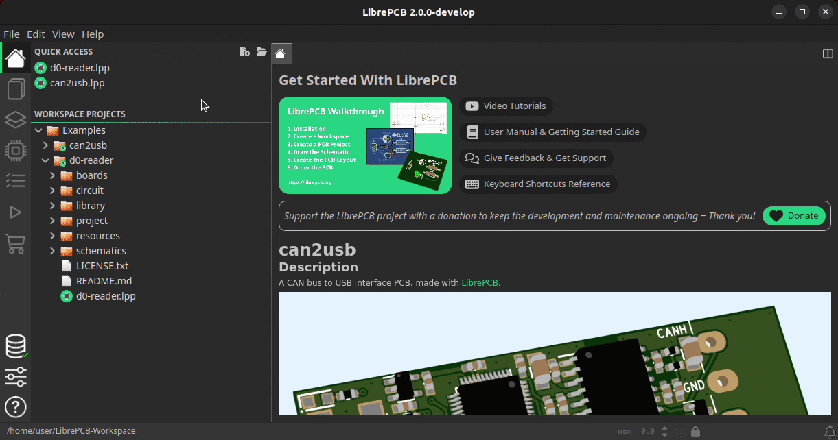
The most obvious change in this release is the new user interface which was built from scratch with the Slint UI framework. It looks very different to the old UI, but the main reason for this change is to improve the user experience and productivity in several ways:
-
Less windows, no more wasting time to switch between multiple windows
-
Less modal dialogs & message boxes which interrupted the workflow
-
Split windows and tabs for organizing the editors according to your needs
-
Efficient use of screen space to maximize schematic/board working areas
-
Clean & simple UI for the simple tasks, but also provide advanced controls when desired
-
Provide hints and guides to make the UI self-explaining
Basically we have replaced 5 separate, single-purpose windows by a single multi-purpose window. In that window you can have as many projects and libraries open as you like, and in every tab you can work on a different task. You can display the board next to its schematic, the 3D board viewer next to the 2D board editor, or compare the schematics of two different projects side-by-side. And on a multi-monitor setup, you can open multiple of those windows which are all equivalent in functionality.
Library Manager
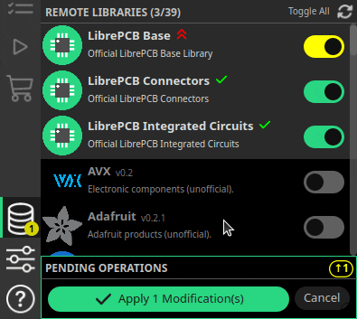
The library manager and the library editor are now also integrated into this new window. The library manager has been rewritten from scratch to heavily streamline the user experience.
The sidebar now even automatically notifies you about outdated libraries, so you don’t miss library updates anymore.
PCB Ordering
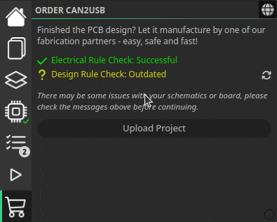
The PCB ordering feature has been rewritten from scratch too and is now integrated seamlessly into the main window.
It now automatically checks the ERC and DRC and warns about outdated DRC messages before you place the order. The days are gone when we ordered faulty PCBs because we forgot to run the DRC!
Schematic Buses (#1646)
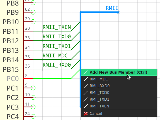
On our user feedback survey, schematic buses are on rank 3 of the most requested features. Now we can remove that feature from the wish list since it has been implemented. All the basic functionlity is there, and more advanced functionality might be provided in upcoming releases. With buses it is possible to group multiple wires in one thick line, called bus, to keep the schematics clean and readable.
Images in Symbols & Schematics (#1578)
Ever wanted to add a diagram, formula, table or simply a company logo to a schematic? This is now possible — just paste any image from the clipboard into the schematic (or load it from a file) and scale/rotate it as desired. Almost every image format is supported, including SVG, PNG and JPEG.
Individual Pads in Boards (#1596)
It has always been strange that pads (whether THT or SMT) or plated slots could only be added to a board indirectly as part of footprints, i.e. through the library system — interestingly not only in LibrePCB, but also in other EDA packages.
But sometimes we need individual, specialized pads or slots in boards e.g. for mechanical purposes, where footprints make no sense. In LibrePCB 2.0 this is now possible. Just add pads or slots to the board the same way as in the footprint editor.
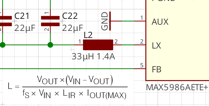
Advanced Design Rules (#1610, #1611, #1606, #1608)
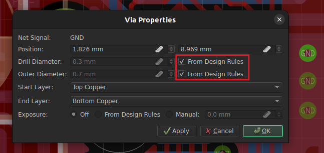
Also noteworthy are some improvements regarding design rules. It is now possible to define the default trace width and via drill diameter in the board settings, so you don’t need to specify those properties anymore when adding traces and vias to the board. And thanks to the automatic via annular ring calculation, you never have to worry about outer via sizes anymore!
In addition, planes allow now to specify separate clearances to copper, board outlines and holes.
Predefined Design Rules & Output Jobs (#1631)
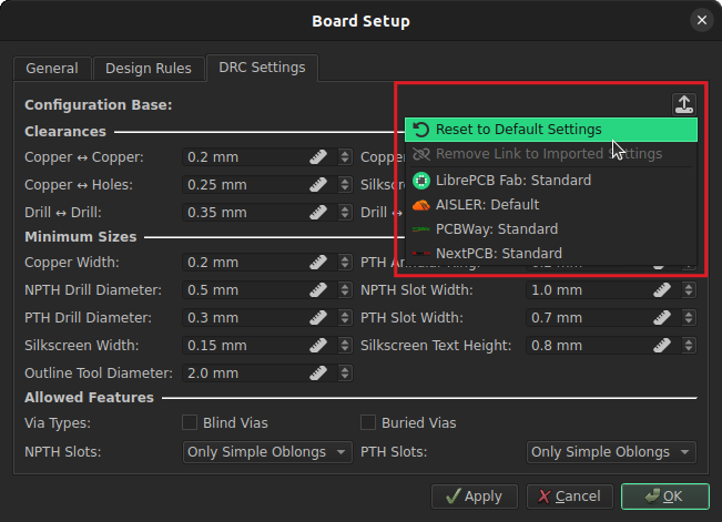
Have you ever entered all design rules according to the capabilities of a particular PCB manufacturer? Probably not, as it is very cumbersome…
With LibrePCB 2.0 it is now possible to store design rules in a library (within so-called organizations), which are then available to be applied to boards. So you can store the design rules of your PCB manufacturer in your local library, and load them into your boards later.
But the real advantage of this approach is that we can now deploy design rules through our library manager! Just install the LibrePCB Base library and you will benefit from the design rules we will add in future.
And this features goes even one step further. In addition to board design rules, it is also possible to share output jobs through this system. So instead of fiddling around with Gerber/Excellon file names in every new project, just load the predefined Gerber/Excellon settings for your PCB manufacturer in a second!