Some of my readers arrived at this substack because I built Investmap, a graph mapping more than 450 companies and 30 checkpoints in the semiconductor industry. I've received feedback on how this tool is helping some of you better understand the industry, so today I bring you something new!
Nowadays the AI buildout is constrained by how fast bytes can be moved around. Training a large model or serving inferences means thousands of GPUs in one building talking to each other constantly. Inside each server, those signals travel over short copper traces from the switch chip out to optical modules at the edge of the rack, then convert to light, then cross the building as fiber-optic pulses. The copper that enables this has been hitting physical limits in different ways: signal integrity collapses, power consumption from copper traces eats a third of the switch’s energy, and the physical edges of the board run out of room for more pluggable modules.
So what’s the solution? Move the optical engines into the same package as the switch ASIC, millimeters from the silicon doing the work. This architecture is called Co-Packaged Optics, or CPO. First production deployments begin in the second half of 2026 with Nvidia’s Quantum-X switches built on TSMC’s COUPE packaging platform. Broadcom follows shortly after. A few months ago, Microsoft also hedged the same problem with a parallel architecture called MOSAIC, which uses microLEDs instead of lasers and was announced in March 2026.
You probably know Lumentum and Coherent. Nvidia paid them around $4 billion combined in early 2026 to lock up their laser capacity. But have you heard of the companies upstream of them? Every silicon photonics chip in production today sits on a wafer made by Soitec, a French company spun out of a government lab in 1992 that still holds about 3,500 patents on the process. Around 60 percent of the world's indium phosphide wafers come from Sumitomo Electric, a hidden monopoly inside a Japanese industrial conglomerate founded in 1897 that mostly makes power cables and automotive wire harnesses. The MOCVD reactors that grow the active laser layers on indium phosphide are 70 to 90 percent supplied by Aixtron in Germany and the hybrid bonder that joins the laser die to the photonic chiplet at sub-micron precision is made by BESI in the Netherlands.
Today I am releasing an interactive map with more than 90 companies involved in this shift in how data moves around datacenters. Roughly fifteen specialist industries have to coordinate to build a single co-packaged module, and at least six of them have one dominant supplier with no real second source. If you want to understand AI infrastructure between now and 2028, you have to understand these companies.
I hope the map below is useful for your learning!
Click here to access the Co-Packaged Optics supply map.
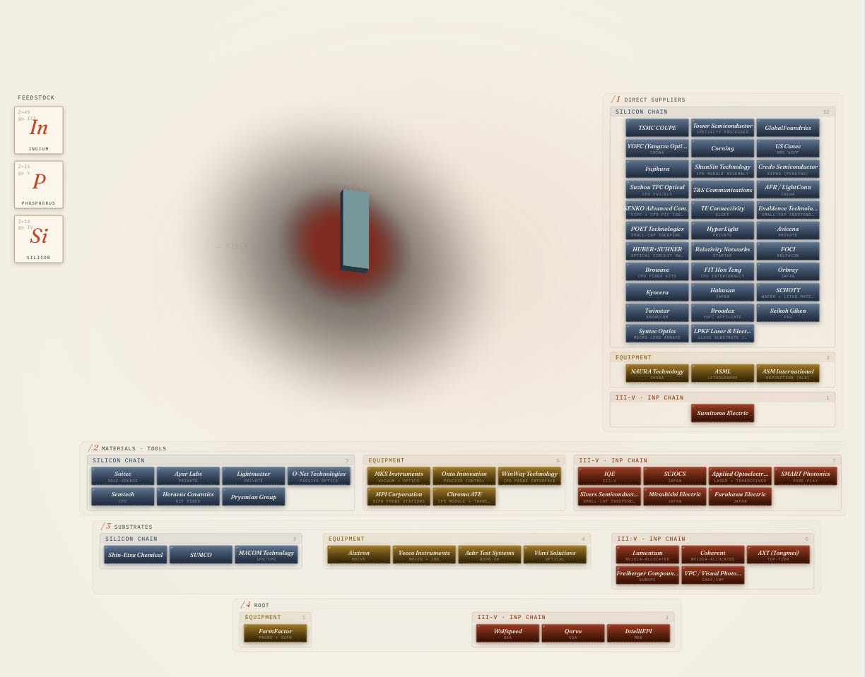
On desktop you can click any part of the CPO and it will show the companies. For the mobile version, I recommend using the buttons at the bottom of the screen. The phone version still needs a bit of polish, which I’ll try to do as soon as time allows.
Using this is absolutely free, but building it wasn’t. It takes a lot of my time and research, so if you can share it with people who might find it interesting, I would appreciate it tremendously and it would help me keep delivering this kind of tool.
If you have any comments, or if you think this kind of thing could be useful for your work, don’t hesitate to contact me. The best supply chains aren’t built alone.