For the past couple of days, I’ve been working on an improved version of the phosphorescence detector circuit. My goal is to improve the device’s sensitivity and reduce signal settling time, so that we can make more precise measurements of faint and extremely short-lived phosphorescence — and hopefully, publish some interesting results.
A major factor that limits photodiode performance is the fact that the device resembles a capacitor; the diode’s parasitic capacitance gets in the way of amplifying signals that are changing rapidly. Luckily, there is a really cute trick that makes the problem disappear. The technique, known as bootstrapping, is outlined in a couple of application notes published by Analog Devices; that said, I don’t think it’s explained anywhere on the internet in a satisfying way. Let’s give it a try!
The article assumes familiarity with signal amplification, photodiode physics, and the dynamics of op-amp feedback loops. If you need to jog your memory on any of this, check out the linked articles before diving in.
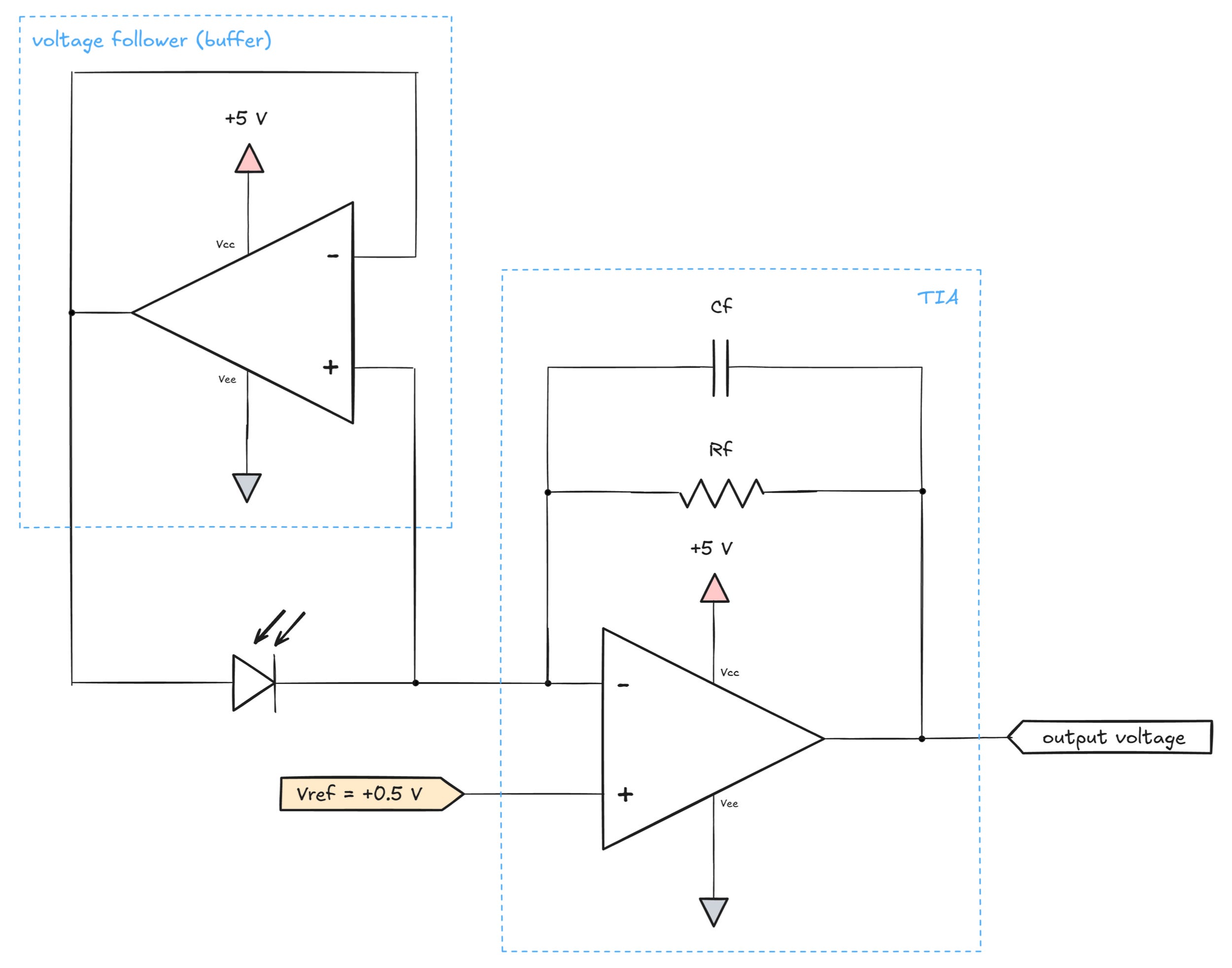
Several posts ago, we talked about a fundamental photodiode circuit: the transimpedance amplifier (TIA). This device converts the induced photocurrent to an output voltage; a simplified TIA schematic is shown below:

To recap: in the dark, the photodiode does nothing, Rf and Cf are of no consequence, and the circuit settles at Vin+ ≈ Vin- ≈ Vout ≈ 0 V. In the presence of light, the photodiode starts moving electrons between its terminals, making the Vin- leg slightly negative. The difference between Vin- and Vin+ is amplified by the IC, causing the output voltage to rise. This, in turn, creates a difference between Vin- and Vout legs, inducing a current through the feedback resistor. The equilibrium is restored when the current via Rf matches the photocurrent, cancelling out the effect of the photodiode. From Ohm’s law, the larger the value of Rf, the higher the output needs to swing to produce the same current through that path.
The wrench in the works is that any diode — including a photodiode — is essentially a capacitor when in an “off” state: it consists of two pieces of semiconductor with a nominally non-conductive depletion layer in between. Granted, our particular capacitor knows some cool tricks: if you shine some light on the junction, electrons get shuffled from one side to another. But it’s a capacitor all the same; in fact, for larger light sensors, the capacitance can easily exceed 100 pF, so it’s nothing to sneeze at.
Worse, in the TIA circuit, this capacitance appears exactly where we want it the least: it’s a shunt to the ground on the inverting input of the amplifier. This input pin is a part of the negative feedback loop that controls gain; if a capacitor must be charged through Rf before the op-amp can “see” a feedback signal, amplification will get out of whack at higher frequencies.
The simplest fix is to “dampen” the feedback loop with a capacitor marked in the earlier schematics as Cf. The capacitor effectively bypasses Rf at high frequencies, allowing higher currents to flow in response to the same alternating output voltage. This stabilizes the circuit, but at the expense of reducing high-frequency gain: the output voltage doesn’t need to swing as much to match the photocurrent. This means that if we actually want to amplify high-frequency signals, we can’t make Cf too high.
There is a standard formula to calculate the maximum TIA cutoff frequency that can be safely handled by a given op-amp for a specific input capacitance (Cin). If you’re curious, I derive the formula in an earlier article. Otherwise, let’s just crunch the numbers for a hypothetical 50 MHz op-amp, a photodiode with a capacitance of 3 nF, and a 1 MΩ feedback resistor:
\(f_c = \sqrt{f_{GBP} \over 2 \pi \ \cdot R_f \ \cdot \ C_{in} } = \sqrt{50 MHz \over 2 \pi \ \cdot \ 1 M\Omega \ \cdot \ 3 nF} \approx 52 kHz\)
But then, in an old Analog Devices datasheet, I came across this schematic:

This configuration matches the earlier scenario; there’s a 50 MHz op-amp, a 3 nF sensor, and a megaohm resistor — but the bandwidth is supposedly 350 kHz, rather than the expected 52 kHz. How come that adding a (now-obsolete) JFET and a 5 kΩ resistor improved the circuit’s performance seven-fold?
The answer is that the transistor, in tandem with the resistance, forms a voltage follower. From the earlier intro to transistor physics, recall that a JFET is conductive only if the voltage between the gate and either of its terminals is above a certain threshold (in this case, circa -0.5 V). The voltage on the upper terminal is fixed, but the other…
Actually, never mind. We can construct a less icky and more understandable version of this circuit the following way:
Any fast, rail-to-rail FET input op-amps should do; suitable examples include MCP6022 (10 MHz), OPA2323 (20 MHz), TLV3542 (100 MHz), and OPA2356 (200 MHz).
So, what’s going on here? Well, the section on the right is the usual TIA layout. The left-hand portion is a unity-gain amplifier, also known as a voltage follower. Simplifying a bit, it looks at the signal on Vin+ and outputs a verbatim copy on Vout. In effect, it works to keep both terminals of the photodiode at the same potential: if the cathode (right) ever moves up or down, the anode (left) is coerced to the same voltage by sinking or sourcing current through the chip’s low-impedance output path.
In this setup, the photodiode is still free to generate photocurrents — and because the voltage follower’s Vin+ leg is very high impedance, the current still has to flow through Rf before reaching the photodiode’s cathode. This keeps the TIA section working as expected. The anode has a low-impedance path to the supply through the voltage follower’s output, so we don’t need any additional connections on that side.
And here’s the kicker: because the diode’s terminals are always kept at virtually the same potential, the internal capacitor can’t be charged at all; any attempt to create an internal electric field will be countered by the voltage follower. In effect, from the viewpoint of the TIA, the diode becomes a nearly-ideal current source, with all the capacitive bits wished away.
It sort of is! Of course, in real life, the voltage follower will have some input capacitance of its own, and that capacitance is added to the feedback loop exactly where the photodiode used to be. The figure usually hovers around 1 to 3 pF, so it’s much lower than the capacitance of a large light sensor; but for small, lower-sensitivity devices, it could be a wash.
The follower has a finite bandwidth, finite loop gain, limited voltage range, and non-zero output impedance — so there are some input signals it might not be able to respond to in time. That said, because it runs at unity gain and can supply considerable currents, the design performs much better than the vanilla TIA layout.
The “bootstrapped” version seeks to keep the diode’s capacitor discharged at all times by maintaining zero volts across the terminals. A cap that’s always charged to a constant voltage would also work fine; it’s just the charging and discharging process that gets in the way. A reverse voltage across a photodiode can improve its response time or sensitivity, and this leads to an interesting variation of the design:

In this arrangement, there is a series capacitor between the buffer’s output and the photodiode, along with a shunt resistor to the ground. The capacitor prevents DC voltages from passing through, so the buffer no longer sets the diode’s DC bias; it’s set to whatever rail the Rp resistor is connected to. In the schematic above, Rp is hooked up to the ground, but we could just as well put it at -10 V.
The capacitor in tandem with the resistor form a highpass filter; as long as Rf ≫ Rp, the cutoff frequency for the follower’s meddling in the diode’s charge state is given by the standard RC formula:
\(f_c = {1 \over 2 \pi \cdot R_p \cdot C_s}\)
The same trick can be used for other capacitor-like signal sources; it’s just that photodiodes need it the most because they tend to deal with high-speed signals, have substantial built-in capacitances, and call for humongous signal gains.
Well, that’s it. Mash that “like” and “subscribe” button to stay up to date on more capacitor and photodiode news!
👉 For a photodiode murder mystery, click here. A thematic catalog of posts on this site is here.
I write well-researched, original articles about geek culture, electronic circuit design, algorithms, and more. This day and age, it’s increasingly difficult to reach willing readers via social media and search. If you like the content, please subscribe!