Irrational Analysis is heavily invested in the semiconductor industry.
Positions will change over time and are regularly updated.
Opinions are authors own and do not represent past, present, and/or future employers.
All content published on this newsletter is based on public information and independent research conducted since 2011.
This newsletter is not financial advice and readers should always do their own research before investing in any security.
Feel free to contact me via email at: irrational_analysis@proton.me
Parametric yield is possibly the worst understood concept within semiconductors. It’s frankly surprising how many people work in this industry and are either clueless or have a very wrong view on how parametric yield works.
Clock speed, power draw, and final product-level yield are an economic choice, not a design choice.
Important background information is available here and highly recommended as a pre-requisite if you want to understand the technical matters properly.
For this post, I will attempt to abstract out the technical details and keep things practical and intuitive. Will heavily rely on public examples and obfuscated first-hand experience. Sections 6.d, 6.e, and 6.f of the old PDK technical deep-dive are of particular interest.
(please please read the old post it will help you understand this one so much)
This parametric yield deep-dive has been sitting in drafts for over a year. Given that Cerebras is such a hot topic, I bumped this one to the top and re-wrote large portions around their chip.
Parametric yield is an industry-wide issue. Cerebras is disproportionately effected by this problem.
Understanding why Cerebras is disproportionately harmed by parametric yield and how they could mitigate this problem is key to understanding the stock.
I would argue it is the only thing that matters for the next 12-18 months for them.
Before jumping into the content, I want to finish this intro with a fun story.
Two years ago, I managed to weasel my way into the private launch briefing for WSE3 with the help of a friend. It took place on March 12th, 2024 at Colovore, a local Bay-Area colocation hosting provider Cerebras used for some of their capacity at the time.
I have been a huge fan of Cerebras since 2019. To be able to see the new WSE3 in real life was so exciting. Took a day off from dayjob to attend. Here are some of the pictures I took.
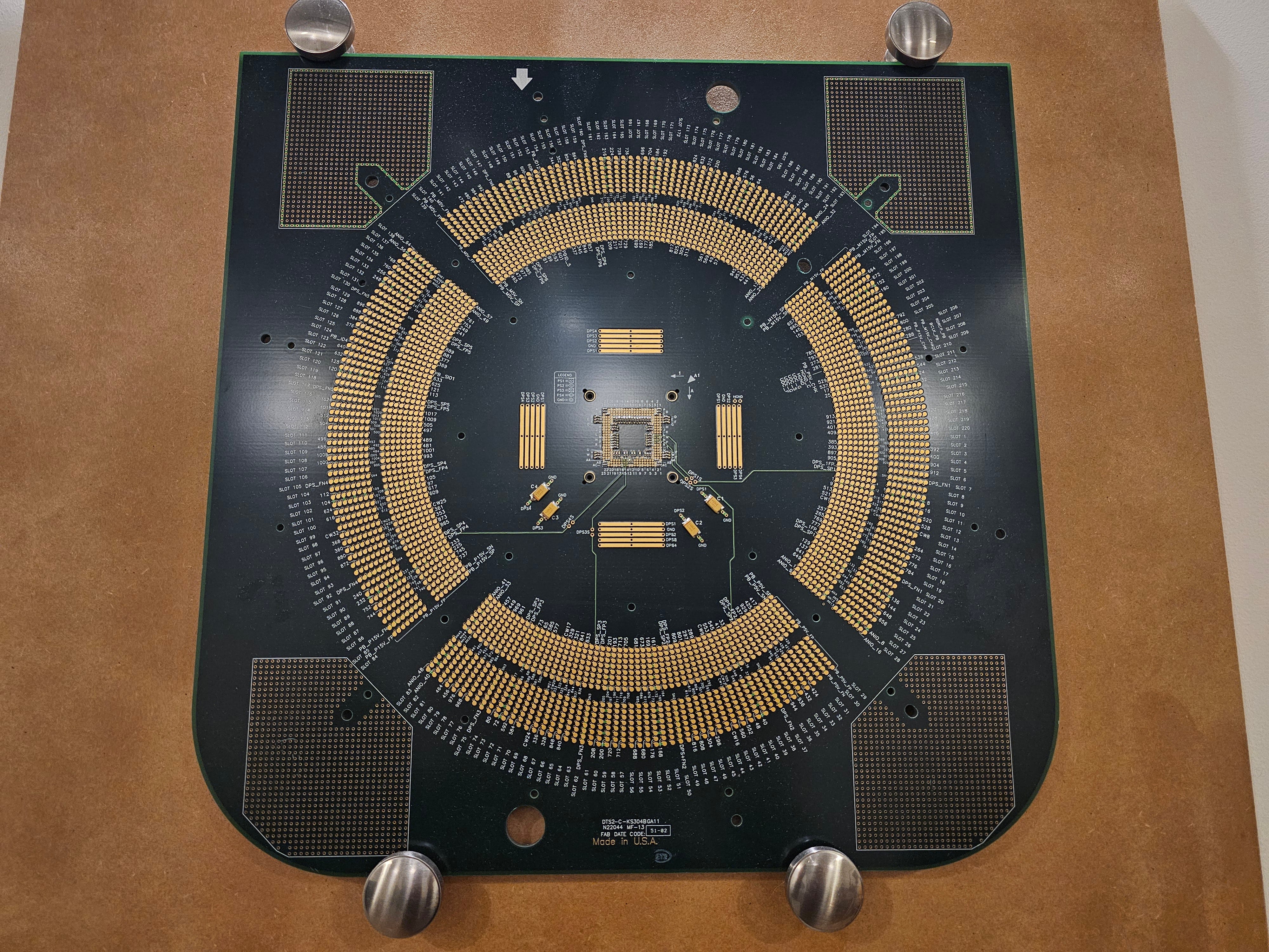
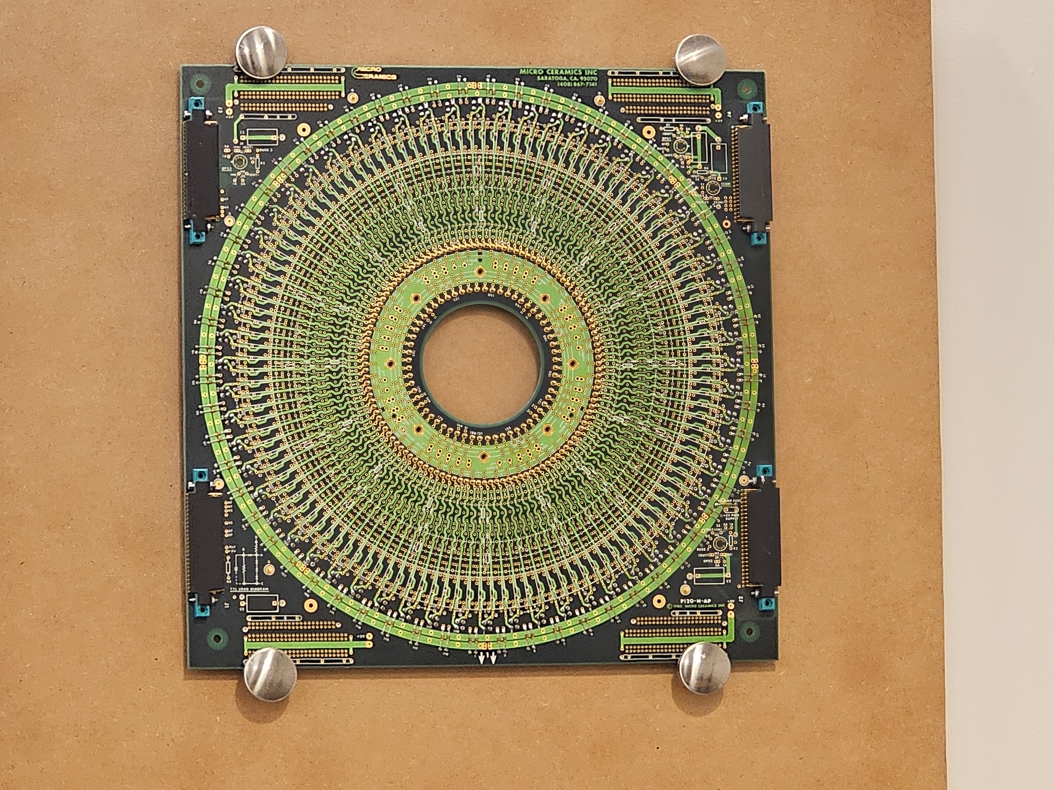
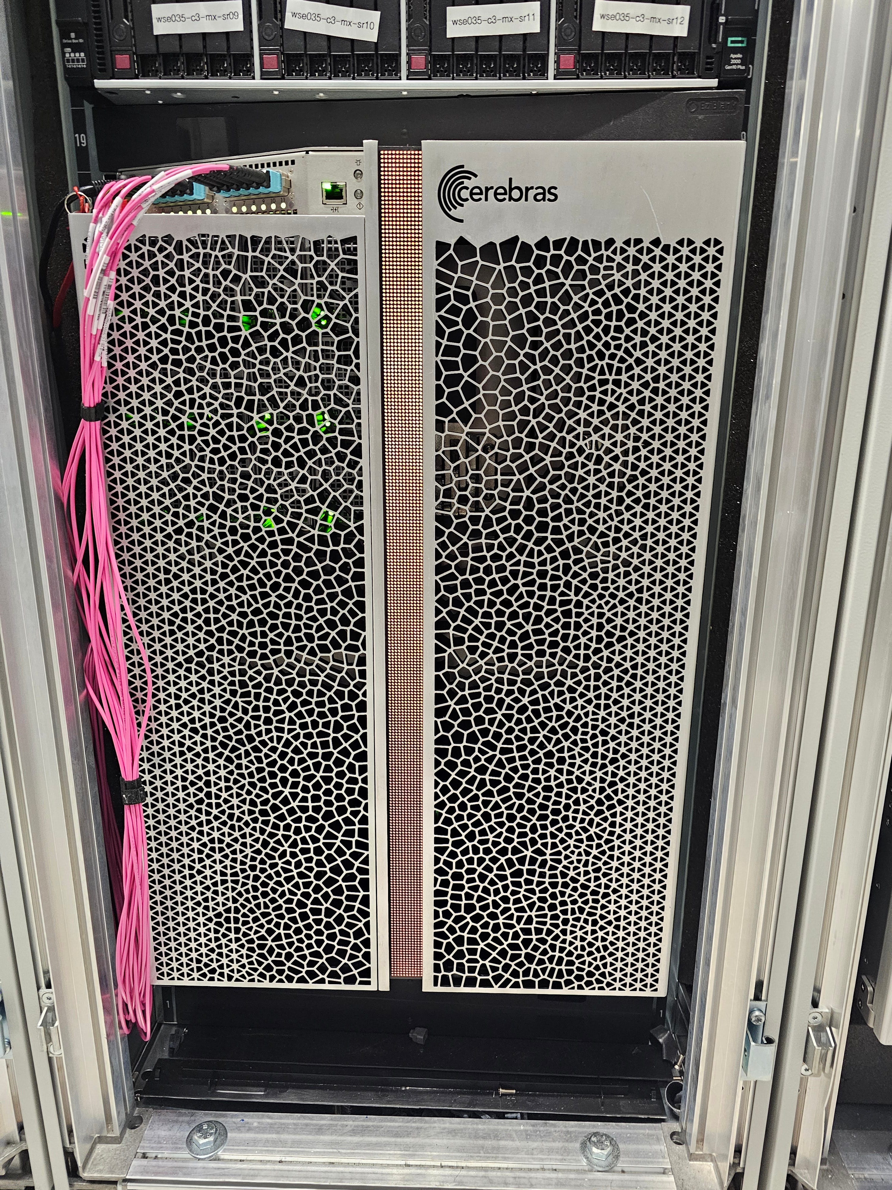
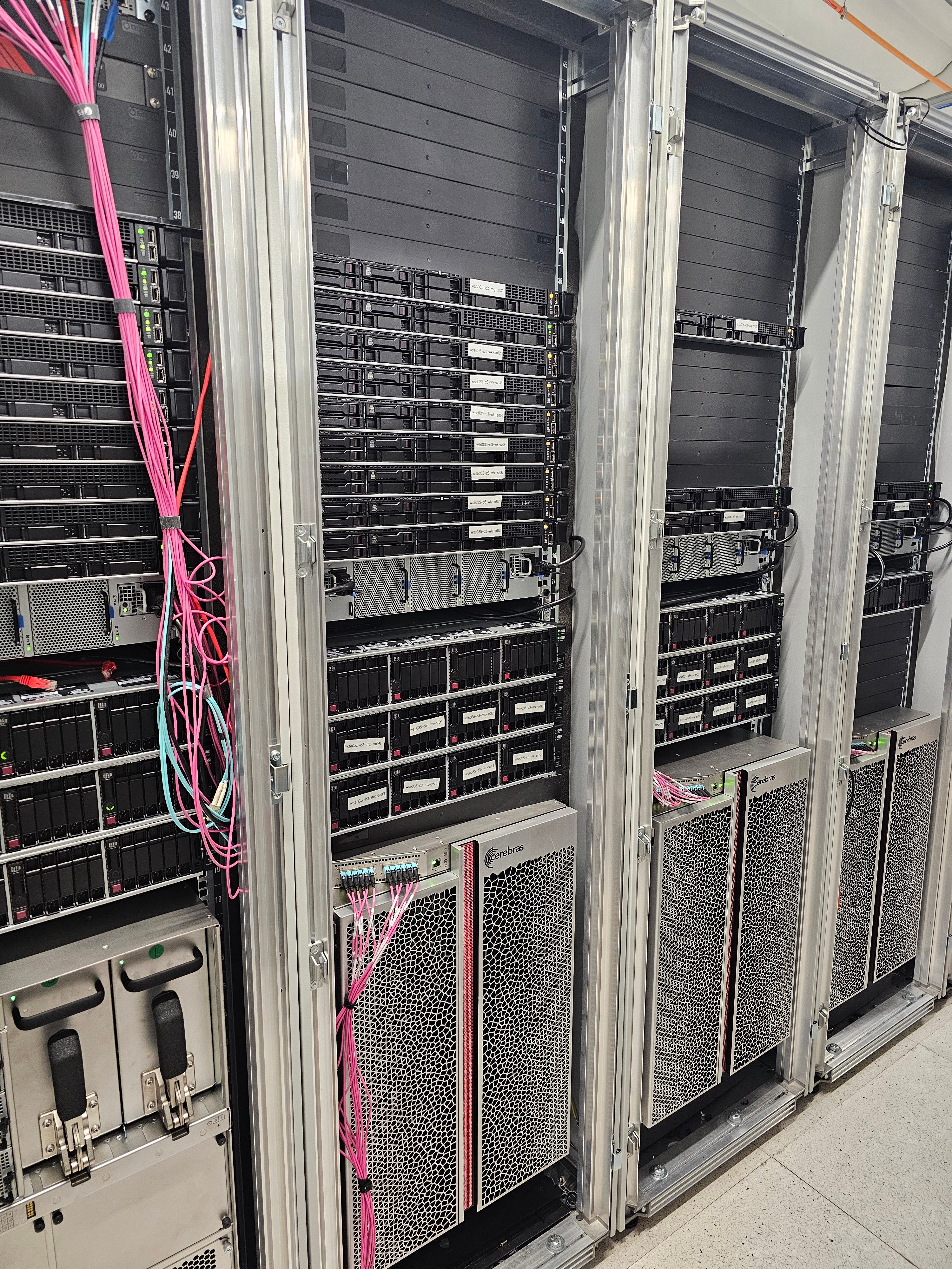
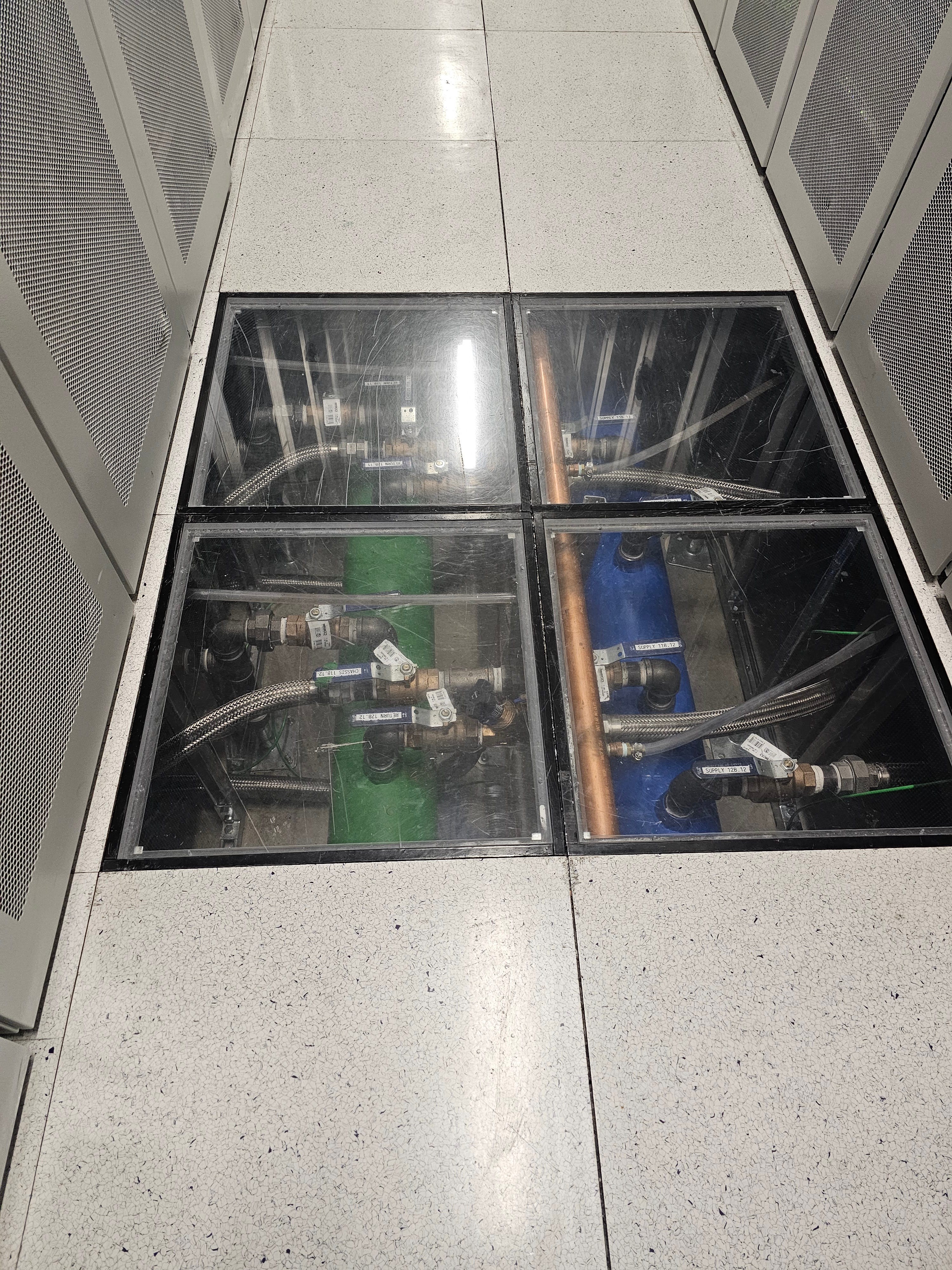
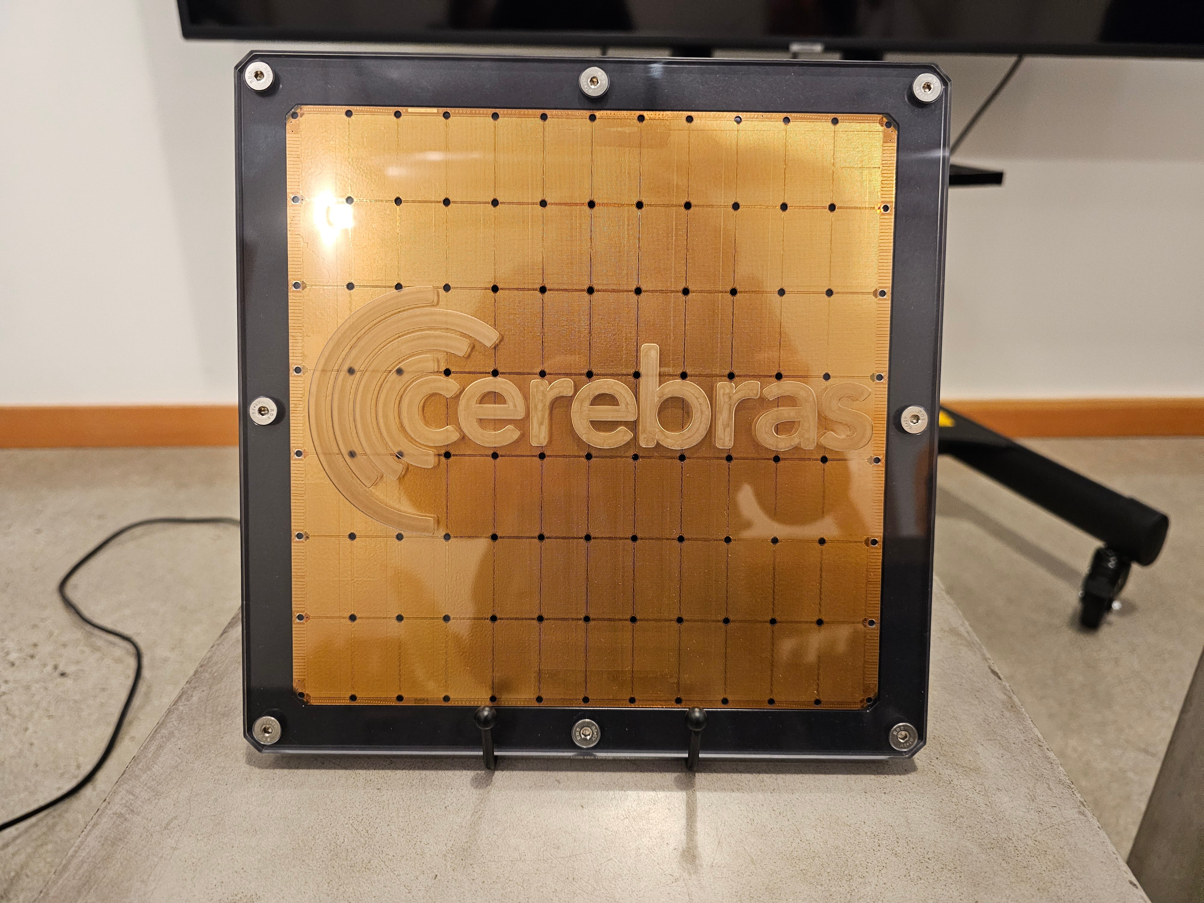
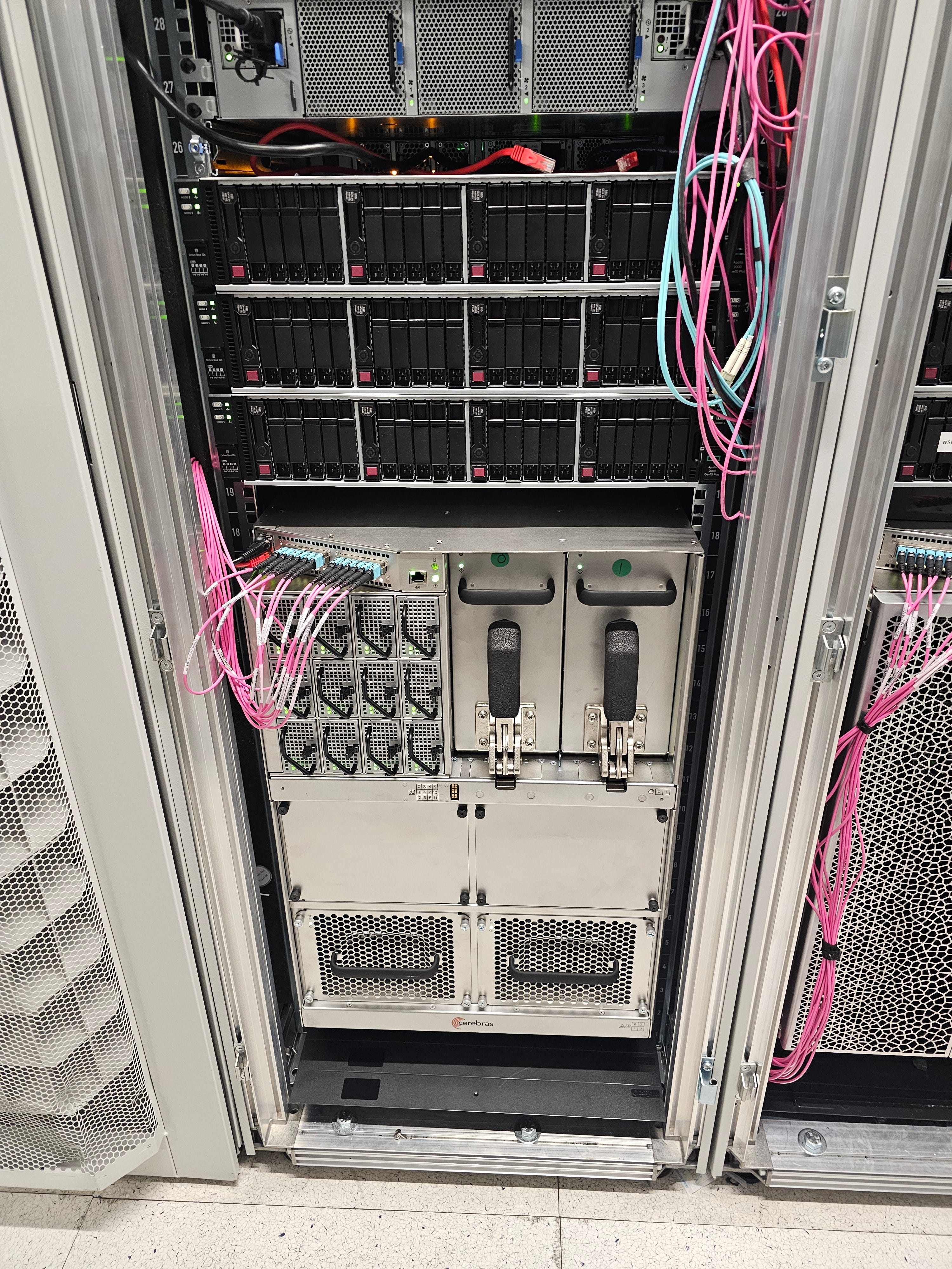
I went into this event as a superfan but left somewhat depressed and concerend.
The WSE3 was a little underwhelming. A minor update.
What concerned me was the vibes. Andrew Feldman looked genuinely exhausted and somewhat demoralized. The Bloomberg reporter absolutely roasted Feldman. It was kind of funny but mostly sad and painful to watch.
One week later (March 19th, 2024) Cerebras held their 2024 AI day (public launch event) as a “me too hey we exist” parasite event in parallel with GTC. That event was a fucking disaster. Concentrated loser energy. Every 5-10 minutes someone on stage would say something so pathetic, I wanted to get up and leave. Unfortunately, chose a seat that made early escape from copium huffing therapy session impossible.

A few months later, someone gave me slides that indicated Cerebras was trying to raise and had failed. This failed round is why the G42 deal+option happened two months later.
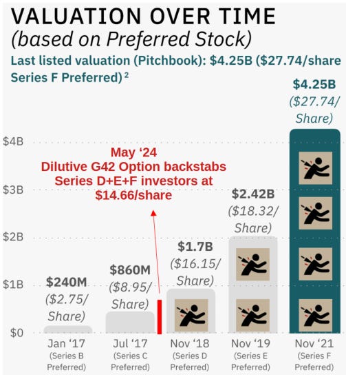
This chart in particular from their March 2024 pitch deck is hilarious.
Anyway, it was around summer 2024 that I had no choice but to conclude that one of my favorite semiconductor companies was dead.
And yet, here they are today, very much alive.
Cerebras is perhaps the most controversial semis/AI stock at the time of writing. I have friends who have large short positions and large long positions. Some contacts have small long positions but keep asking me for advice on if they should size up and make Cerebras a big position. Other contacts have no involvement with Cerebras and just shit on them because they think Nvidia or various startups are better.
I would like all of you to set aside your biases, both positive and negative.
Try to be fair and balanced like me.

What if Cerebras the product is good, but the supply is very bad because parametric yield very bad?
Can they fix parametric yield problem and make supply good?
The real world is Gaussian.
Real-World Public Examples
Corners and Dartboards
Economic Choices
DVFS and TDP
Be first, be smarter, or cheat.
Cerebras unique situation, and possible outs.
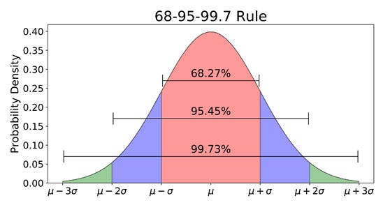
Semiconductor design and manufacturing depends on a lot of very complex physics/chemistry and material science phenomenon. And yet, this is all abstracted out in the process development kit (PDK).
From a designers perspective, the real world (litho, etch, deposition, … variation) changes the numbers/attributes of core building blocks (devices). Transistor gate threshold, leakage power, rise time, capacitor parasitic resistance (ESR), ….
All end up as numbers in their own normal/Gaussian distribution.
Variation is natural. In order to maximize parametric yield the following typical flow is followed within industry.
Design simulates and margins circuits (analog+digital) at +/- 2 sigma process variation.
The leading-edge logic Fab (TSMC, Intel Foundry, Samsung Foundry) produces a special lot of chips called the characterization lot. These chips are run through the manufacturing line slowly and intentionally over/under doped so the process corner (+/- 2 sigma variation) is known a-priori.
Post silicon validation (my job) takes the characterization lot and figures out a unified set of default configuration parameters such that all corners pass.
Mass production begins where the process corner off each chip is not known a-priori.
Assuming everyone did their job correctly, parametric yield will be ~95%. This is the yield after defective (catastrophic yield) chips are discarded.
Of course this is over-simplified. Voltage and temperature play a huge role. This is why the acronym PVT (process, voltage temperature) is used. But as a general idea, this is how semis work in the real world. Everyone is fighting the same problems which manifest themselves as Gaussian/normal distributions.
I think it would be helpful to cover some real examples to build your intuition before going further on the technical side. Just by looking at the SKU stack of major semiconductor companies you can see parametric yield in action.
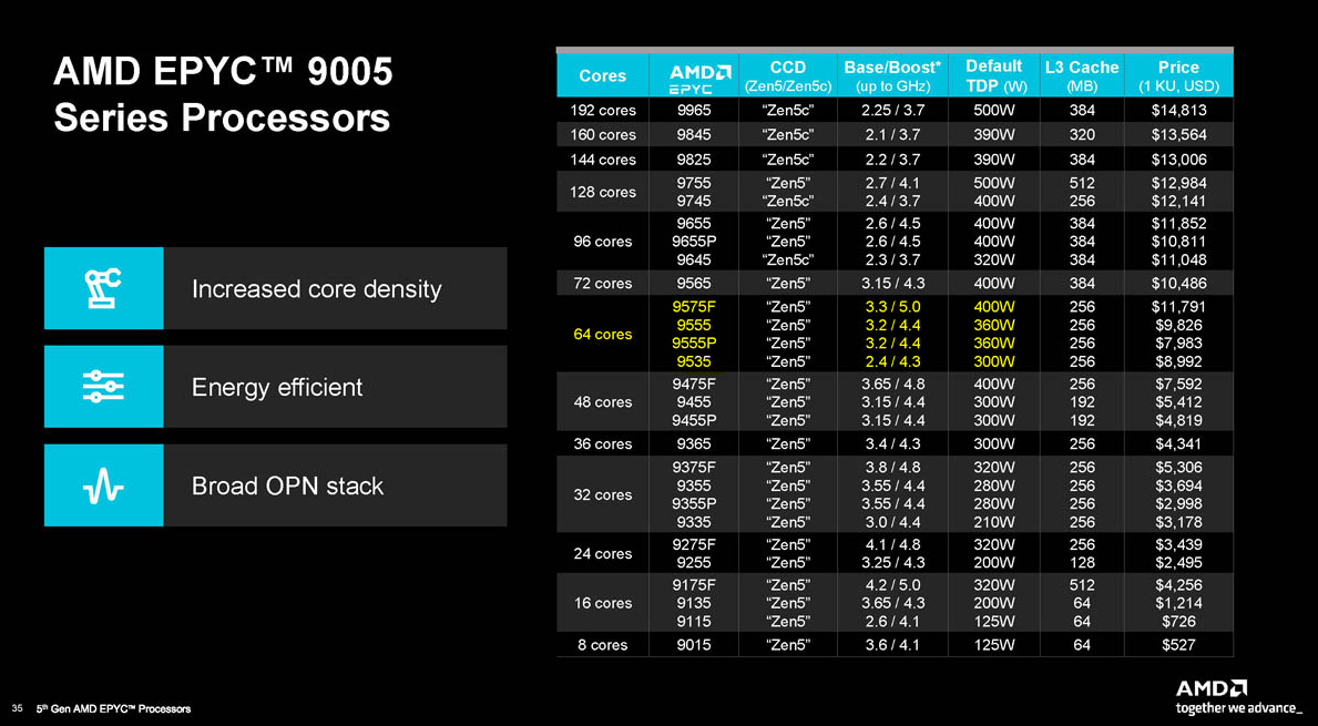
AMD offers four 64-core SKUs within the Turin family.
Each has a slightly different base clock (minimum speed for each of the 64 CPU cores) and boost clock (highest speed of all CPU cores assuming thermal limits are not hit). The power draw also varies quite significantly. 33% more power in the 9575F versus the 9535.
The silicon in all these products is the same design.
What makes them different is parametric yield, not catastrophic yield.
Catastrophic yield (defects, defect density) already determined how many cores are alive. Parametric yield determines how fast the cores run and how much power they draw.
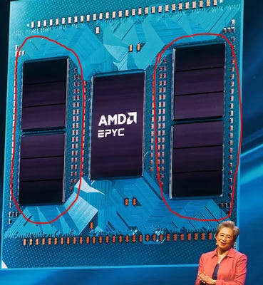
You can think about this in terms of Gaussian/Normal distributions. Made up numbers because this information is closely guarded secret internal to every company….
Suppose only the top 30% of CPU core chiplet dice are “high enough quality” to make it into a high-frequency 9575F. Obviously throwing away the other 70% would be bad, so make slower/cheaper products like the 9535 with those.
This concept is called “yield harvesting” and is very common within semis. Let me show you some more examples.
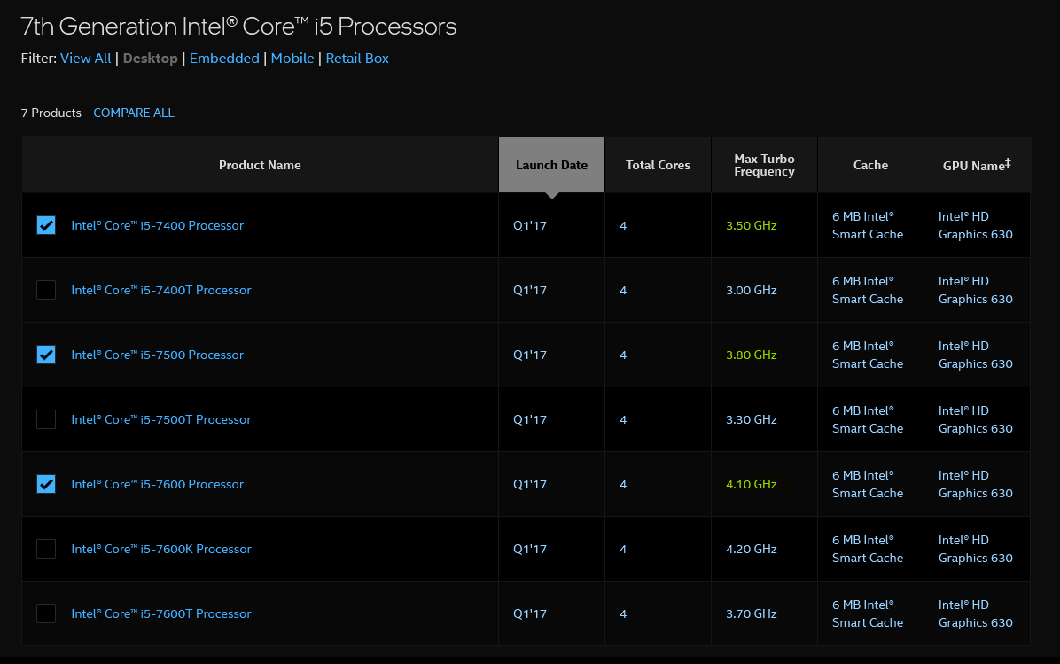
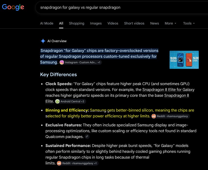
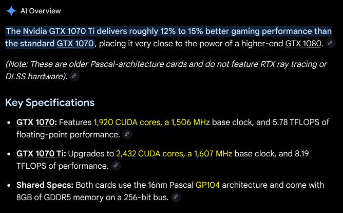
Nvidia’s gaming department (RIP does anyone care about them these days lol) has a tradition of releasing a “TI/Super” version of each GPU model around 6 months after the normal versions launch. TI/Super models are just higher bins, both in cores enabled and frequency. They need time to build up stock of the top X% of chips to supply the higher-end SKU.
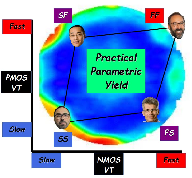
Process corners look like this in chart form.
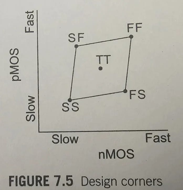
The two types of transistors (N/P[MOS]) have varying speed in a Gaussian distribution, as all natural things should have.
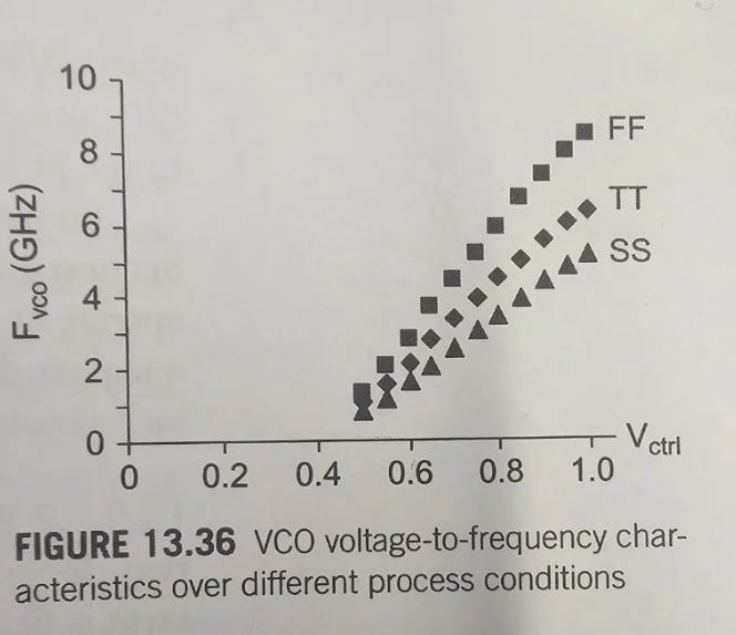
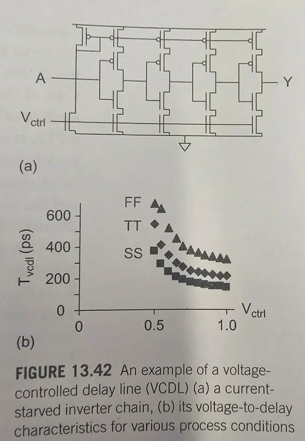
Fast corners are… faster (obviously) but also kick out way more heat due to worse leakage power. So congratulations, your FF parts have a much easier time hitting target clock speed but overheat. I intentionally chose to make Gavin Baker the FF corner in thumbnail. Please clap at this clever detail.

Process corners are typically at +/- 2 sigma as a reminder.
Voltage is typically simulated at +/- 10% with respect to nominal but characterized at +/- 5%. In some cases companies choose to characterize at +/- 3% and require customers to design better power delivery to account for the tighter quoted tolerance. But designers always simulate at +/- 10%.
Finally we have temperature where there is a lot of variation depending on the company and product end market.
Standard corners are -20C and +110C.
Extended corners (automotive, industrial, military) are -40C and +125C.
A popular reduced range is 0C to 70C or 90C.
Imagine all of this corner stuff as a dartboard.
High-volume manufacturing is the logic Fab throwing darts while blindfolded. The system integrator (entity that buys the chips and makes motherboards, racks, laptops, smartphones, whatever) is responsible for power delivery and thermals. They too have their own dartboard due to variation in power delivery components and thermal/mechanical tolerances.

If you build millions of something complex, there will be meaningful variation. The trick is to bake enough margin across the stack (PVT) such that your parametric yield (and thus economic outcome) is economically optimal.
I find it very irritating when people take engineering sample leaks as gospel.
At what corner is that engineering sample from…? You don’t know? Well then shut the fuck up this is useless information.
At the end of the day, clock speed is a choice, not by the designers.
This trips a lot of people up. It seems a lot of people have an intuition that designers target a clock speed and that is the goal.
In reality, clock speed is an economic/business choice. Post-silicon validation figures out what reality looks like and product management (business group) decides the final clock speeds and SKU stack.
Sometimes things go wrong. Two famous examples are AMD RX Vega (which got Raja Koudori fired from AMD) and Nvidia Ampere Gaming (RTX 3000 series).
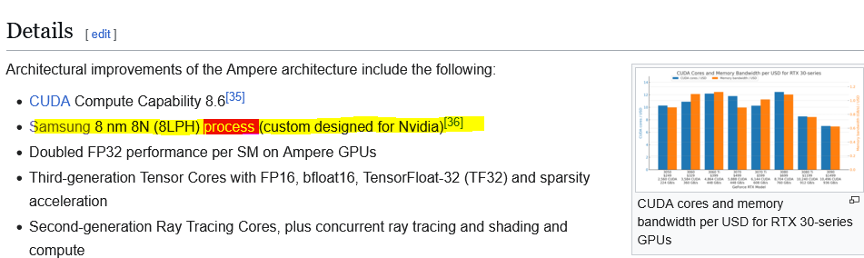
To understand what happened with these two product lines, you need to understand these two charts.
First, the Schmoo chart.

More voltage means more heat generated. Every chip has one of these curves.
The same data can be plotted like this.
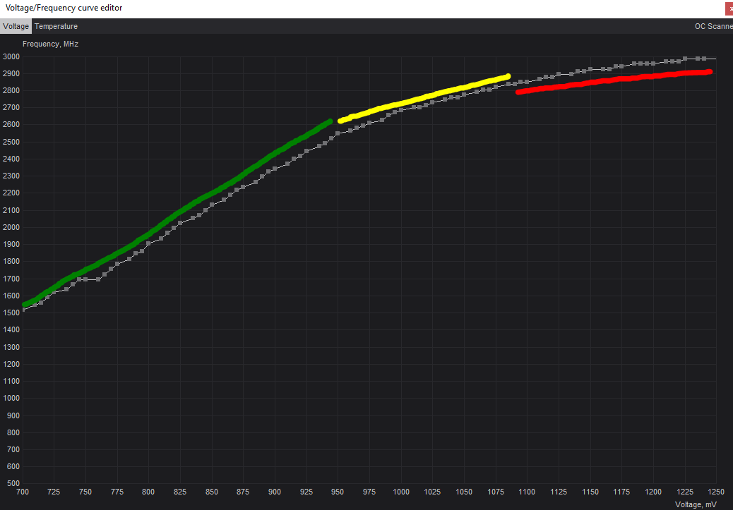
In general, most chips have this three-region response in voltage versus frequency.
First a linear region where you get good gains. Then a region where there are diminishing returns. Finally a region where you shove huge amounts of power and get almost nothing for it.
In general, products are targeted at the edge between green and yellow region, with some opportunistic boosting into the yellow region.
What Nvidia Ampere Gaming (3000 series) and AMD Rx Vega have in common is both were factory shipped deep into the yellow region and in some cases into the red region.
Remember, clock speed is a choice. Design, marketing, product management, and competitive analysis groups had a set of goals. Gaussian reality, conveyed by post-silicon validation group, resulted in unexpected changes to the plan.
When reality becomes severely disjointed from the original plan, it means someone fucked up badly. Modern EDA tools are quite good.
In the case of Nvidia Ampere Gaming (3000 series) it was Samsung Foundry’s fault.
In the case of AMD Rx Vega, it was Raja Koudori and his mis-managed design group’s fault.
Dynamic Voltage Frequency Scaling (DVFS) is a very common strategy that has a lot of potential complexity in its implementation.
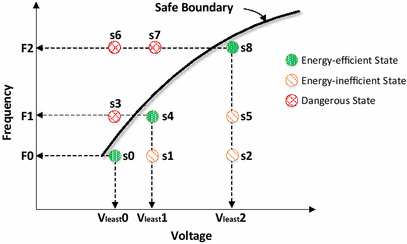
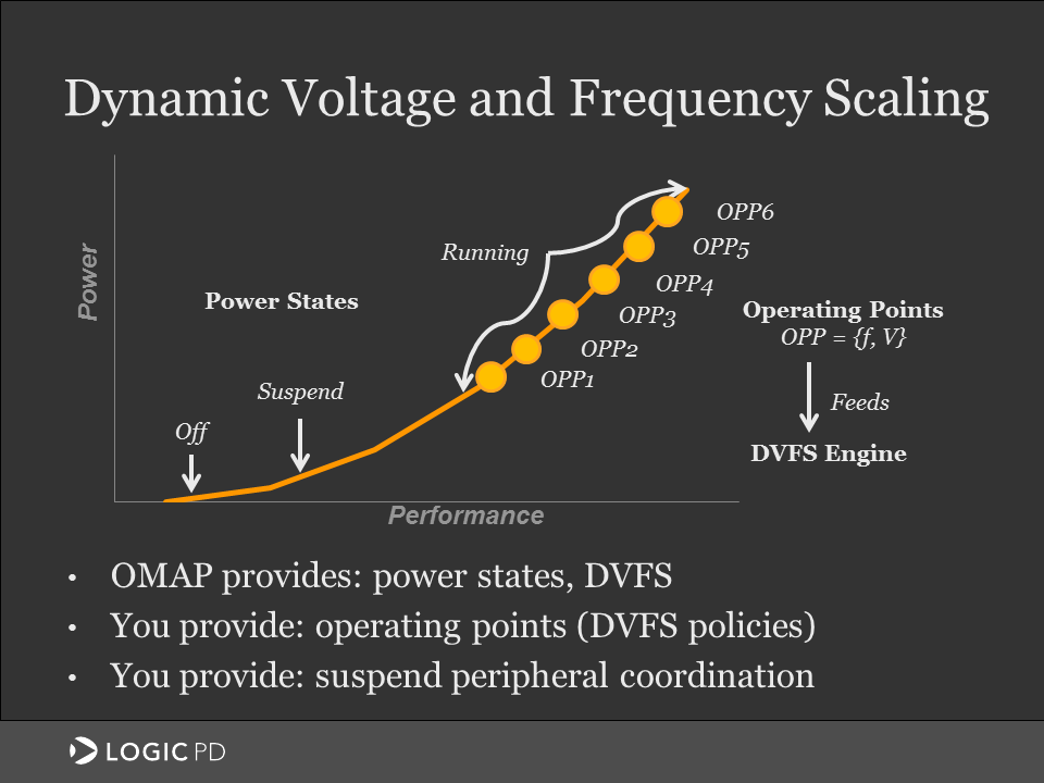
TDP stands for thermal design power. This is the maximum sustained power a chip can draw because the cooling is built around this maximum.
I made “sustained” bold because peak/instantaneous power can (and regularly is) be much higher.
Chips have many internal sensors. Only a small subset of which are exposed to end users. Lots of hidden goodies locked behind encrypted and obfuscated firmware and fused off registers.
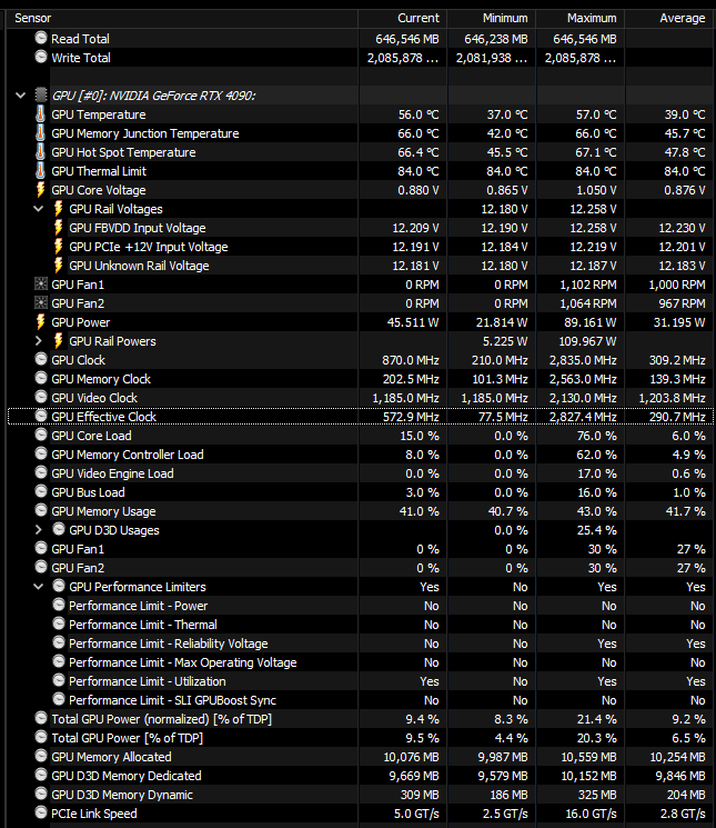
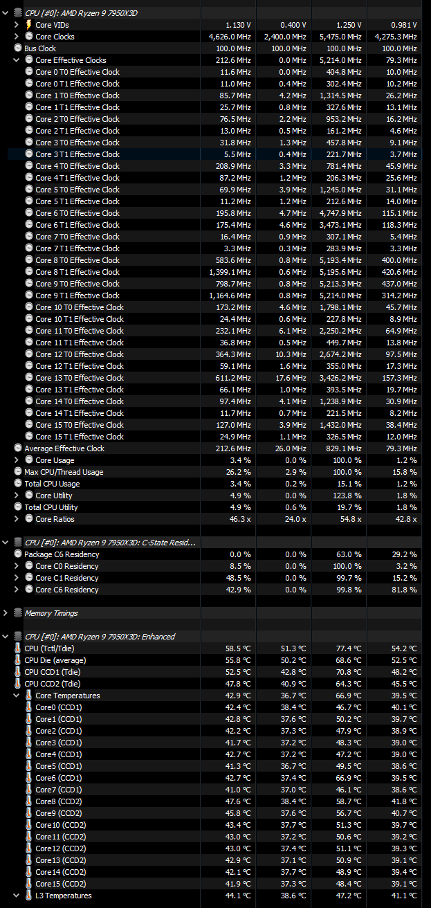
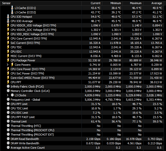
To help build your intuition, let’s look at a generalized scenario.
You have a chip with the following attributes:
TDP of 100W
10 different blocks (CPU core, systolic array, polynomial engine, SIMD engine, whatever)
1000 sensors (temperature, voltage, counters, busy/open signals, utilization, …)
The objective is to maximize performance while staying within sustained power, peak voltage, and thermal limits.
“Maximize performance” could mean absolute performance or performance/watt. Depends on your goal. Often this toggle is exposed to users or at least end customers.
(See Nvidia MAX-Q vs MAX-P)
This puzzle is a lot more complicated than you think.
What if a workload stresses “block X” much more than the other blocks? You will get a hot spot.
What if the system ends up more efficient in a “race to idle” scenario in which DVFS pushes the chip into an inefficient state but for a shorter period of time?
How to allocate power budget across blocks?
And remember… PVT variation (PARMATRIC YIELD) is still around, making this problem much more difficult and varied.

Semiconductors is a ruthless industry. Miss a product window and the competition will cut your throat ear to ear.
Much like one of my favorite Margin Call quotes, there are three ways to make a living in this [semis] business.
Be first.
Be Smarter.
Or cheat.
The thing about semis is, this world is largely self-policed because cheating is very easy and the only way to find out (for sure) if someone lied to you is to get volume samples to independently test.
To understand what I am talking about, let me give you some real examples, some of which are heavily obfuscated for obvious reasons.
Lasers are typically (almost always…) run at 40C die temp or higher. Lumentum’s public UHP demo at OFC 2026 was at 30C. This information was disclosed in their laptop monitoring tool in small font while the headline numbers (optical output power, efficiency, RIN, linewidth) were in big font and on the slideshow TV.
At DesignCon 2025, Marvell had an optical DSP demo (3nm, 1.6T) that had very aggressive cooling.
Same conference, Alpha wave had a PCIe 7 live demo showing 1e-12 BER (very good) but at a relatively short channel. Meanwhile the marketing materials discussed support for much more lossy channels.
There was a time where I was debugging a performance issue and found a register that would juice a small sub-circuit bias voltage and deliver significant performance gains. The overall power draw of the chip and thermal dissipation were the same.
When I shared my results with design, one of them had a visceral negative reaction and demanded I never use this register again. Apparently, it was included as an emergency debug feature. Leaving that register enabled would lead to catastrophic electromigration issues. Essentially the chip would fry itself after a few months.
Think about what this kind of situation enables.
I could have kept that register enabled and lied to my manager.
My manager could have ordered me to use the register anyway for marketing and test reports but disable it in customer firmware. When the customer realizes performance is worse than the report, too late they already committed to purchasing the product and cannot switch.
A single person, even a low-level IC, has the power to commit significant fraud. This is common simply because of how complex semis are and how easy it is to hide things from other internal departments and cheat.
(we did not use the register… took me a couple weeks to find a safe solution)
There was a time when a competitor was telling (shared potential) customers very unsafe and unethical things about undervolting.
As a reminder, designs are almost always simulated at +/-10% and characterized at +/- 5%.
The competitor (same product class, same process node) was quoting -18% voltage as safe and viable.
Marketing and upper management of <former employer> placed enormous pressure. My former manager instructed me on how to safely determine what undervolt we could commit to without being unethical. After a month of work, the result was a -12% or -14% depending on some nuance. My former manager wanted to be safe and decided to pass along power numbers at -10% to be conservative.
Word of advice, this industry is built on reputation. If you are consistently asked to do potentially unethical things its time to find a new job. It will greatly benefit your short-term sanity and long-term career opportunities.
People know who worked at which company on which group/project.

Word gets out.
You will never sell anything to any of these people ever again.
Remember that job interviews are you selling yourself (your labor).
Cherry-picking is a common practice. If a company is demoing some chip at a conference, they are not going to pick an FF or SS part. Of course it will be a TT part.
But suppose you have a tray of 100 TT parts. Are you going to pick a random one?
No… you will pick a subset of TT parts to test and use the best one.
Is testing 5 TT parts and picking the best ethical? Sure its marketing.
How about testing all 100 TT parts?
There exists a line between reasonable marketing/promotion, and cheating.
There exists another line between cheating and fraud.
Do I sound like someone who knows how to cheat and spot cheating? These are highly correlated skills.
One of my (unusual) hobbies is to watch police interrogations. I sometimes copy their strategies. Start with some soft and friendly questions to make the target feel safe. Then abruptly pummel them with sharp, specific questions. Cut them off and don’t give them time to think. Latch on to their mistakes.
You would be surprised at how many people crumble under pressure and give away key details.
This brings me to the 25% B0 Jalapeno clock speed comment by Semianalysis.
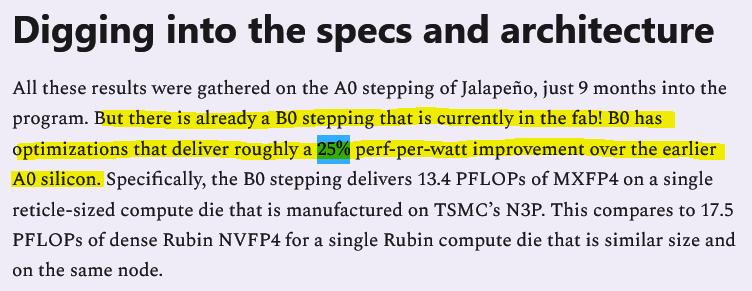
This is an absolutely massive red flag. It’s a red flag that is on fire in an incandescently bright manner.
A 25% delta in perf/watt (optimum point on volt/freq curve) going from A0 to B0 means catastrophic failure. SA passing along this detail without realizing or discussing its significance is a huge miss. This detail is so huge, nothing else matters.
Something went seriously wrong with Jalapeno. As far as I am concerned, A0 is broken and parametric yield must be an unmitigated disaster. This is the opposite conclusion/narrative of SA.
Remember, designs are simulated at +/-10 voltage corners and +/- 2 sigma process corners.
If your clock speed is off by 5-10% (A0 vs B0, or A0 vs target) after characterization and tuning, then that is a modest mistake.
Off by 15% means something severely went wrong.
Off by 25% is a disaster and might as well be off by 50%. Someone fucked up badly in this scenario.
Catastrophic. Failure.
In this case, the foundry is TSMC N3P, the worlds second best leading-edge logic process node and PDK. N5/N4P PDK is worlds best. N3E/N3P had some minor regressions in PDK quality two years ago which have since been mostly fixed.
So either Broadcom fucked up or OpenAI (+ the AI agents who vibe-coded all the RTL in “record time”) fucked up. I will leave it to you to come to your own conclusion on who is responsible for the Jalapeno A0 disaster.
Parametric yield is an industry-wide problem. Cerebras is disproportionately affected.
It’s not their fault. It is a logical and natural consequence of their core technology, wafer-scale compute.
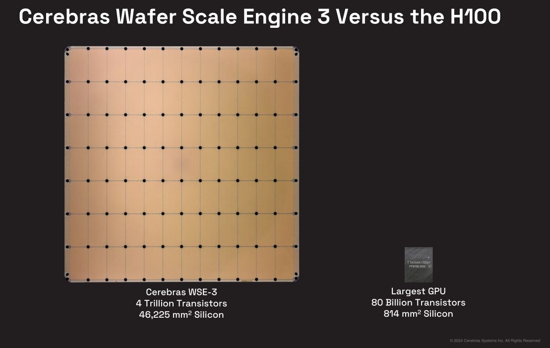
Engineering is about tradeoffs. Nothing is free.
Most AI accelerators are built with reticle-sized dice that can be tested and characterized before advanced packaging. So most of parametric yield and tuning work can be done at a die level. Most, not all. There is some variation in advanced packaging parasitics.
Cerebras has to effectively get good parametric yield on 84 reticles on the same wafer.
Remember, the normal strategy’s every other semiconductor company uses for parametric yield are:
Throw away chips that are too slow or run too hot. (Cerebras can’t do this)
Sell lower quality chips as a different SKU. (Cerebras can’t do this)
Change various registers and settings of each chip to tweak and get most of them to pass spec. (Cerebras might be able to do this in a limited way… more on this later…)
What makes this situation much worst for Cerebras is test flow.
Every logic wafer is tested at a wafer-level using ATE machines (Teradyne, Advantest). This stage of testing is really for basic diagnostics and to find out which chips are healthy enough to package. Packaging is expensive.
System-level (packaged part) testing is absolutely critical for tuning and to figure out which devices are good enough.
The penalty for throwing away a bad (failed parametric yield) packaged GPU/ASIC (normal ones) is bad but not disastrous. Yes it hurts throwing away 1-2 reticle-sized logic chips and 4-6 HBM stacks and some CoWoS-L wafer area. But you can set up a socketed test rig and avoid throwing away power delivery, PCB and other stuff and assembly cost (money and opportunity/time cost) is not that bad. Modern thermal heads and test rigs are pretty good.
Cerebras gets killed by all of this. They have to package the wafer with all the expensive custom vertical power delivery and bespoke cooling into the final product. There is no real test rig. At least no test rig with economics and usability anywhere close to those for normal chips.
You can see this from the OpenAI Jalapeno test rigs.
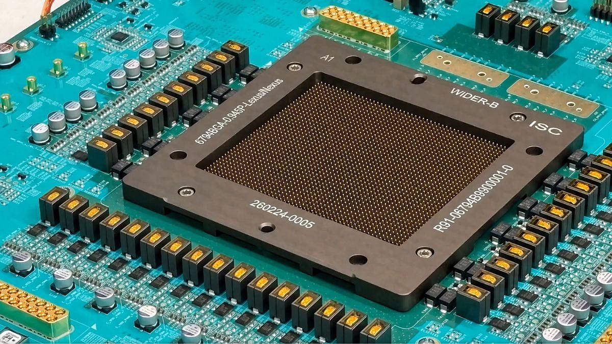
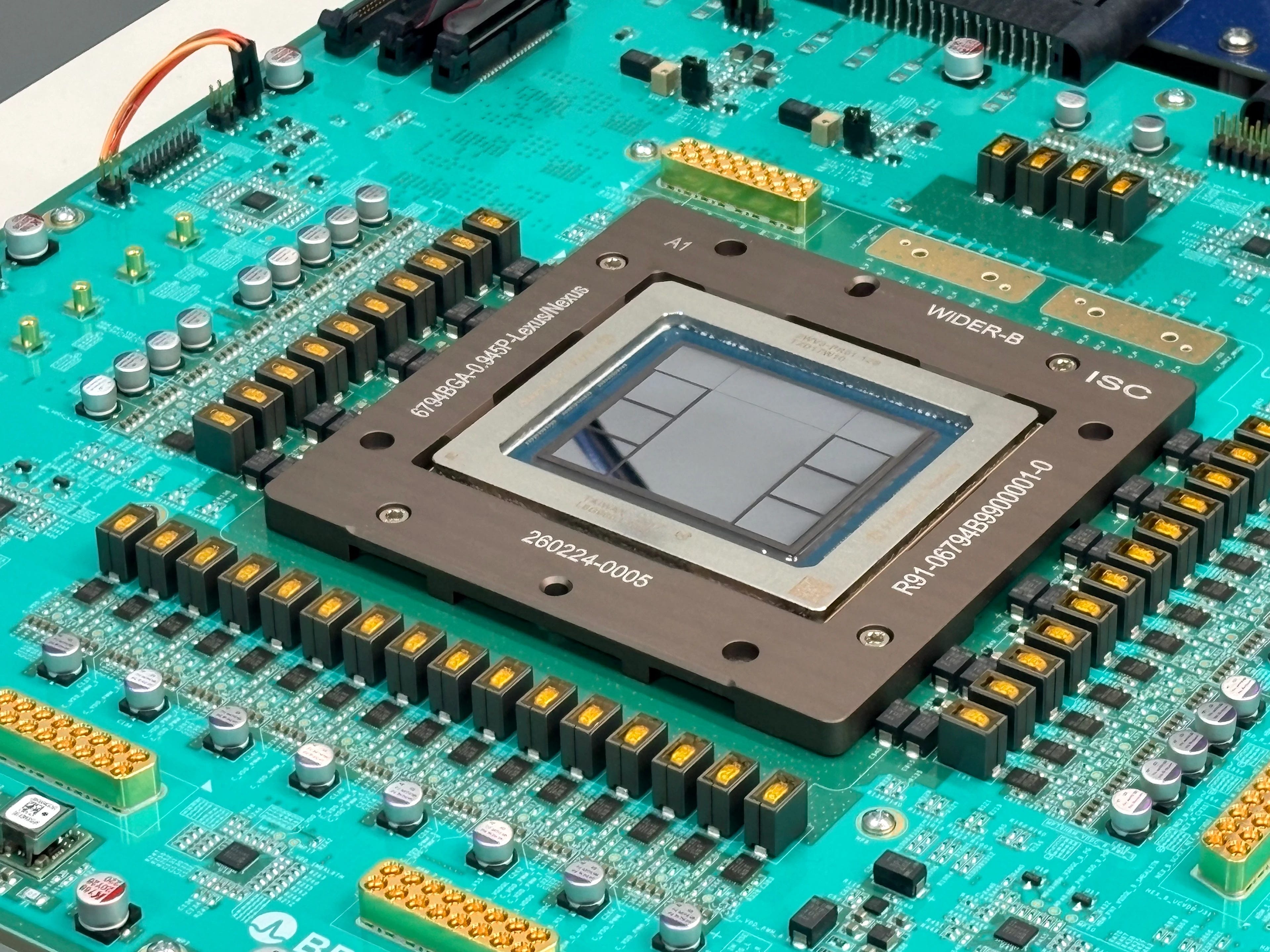
Socketed PCB. Easy access to jumpers and diagnostic pins. Over-built power delivery to run DVFS experiments. Easy IO diagnostics with Samtec Bullseye connectors. And an automated vertical thermal head (not shown, I am assuming) for thermal sweeps.
It matters a lot having the ability to set chips to specific temperatures to evaluate performance and debug timing issues.
Cerebras is so limited in how they can test and deal with parametric yield. It’s a very difficult problem I am not criticizing them. Just pointing out how severe the problem is because of… reality.
I want to frame this section is a particular way.
Cerebras was founded in 2015.
The first WSE was released in 2019.
The current generation WSE3 was released in 2024.
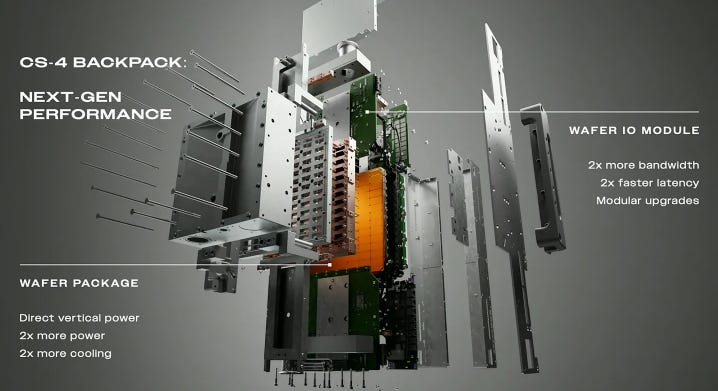
An updated enclosure for WSE3 (significantly better power delivery and cooling) was released in 2026.
Suppose you reduced Cerebras down to 10 “dangerous/existential” problems.
How to get cross-reticle stitching to work?
Vertical power delivery and cooling.
Graph compiler.
…
…
…
blah blah blah.
Obviously, they had to prioritize which dangerous problems to work on. What to fix first and how much effort.
I believe that parametric yield is the problem that has gotten the least attention from Cerebras.
Again, this is not a criticism. These guys had to prioritize and deal with limited resources.
From my conversations with Sean and JP, it really seems like after all these years, they have only just started to seriously look into parametric yield.
One of the most obvious strategies is to give each reticle on the WSE it’s own voltage or even go further and give parts of each reticle their own voltage domain.
Sean has been repeatedly very evasive when I ask about this. My guess is the entire WSE3 has a unified power grid and there is no ability to voltage-tune their way out of parametric yield issues.
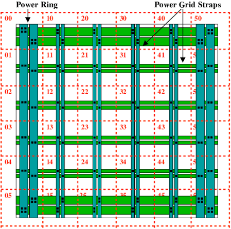
It is very suspicious that the CS-4 (with overclocked WSE3-turbo) doubled the clocks of everything. IO and core clock.
My conspiracy theory is they were operating at a hilariously low section of the volt/freq curve and managed to double because of improved cooling and reduced power supply ripple.
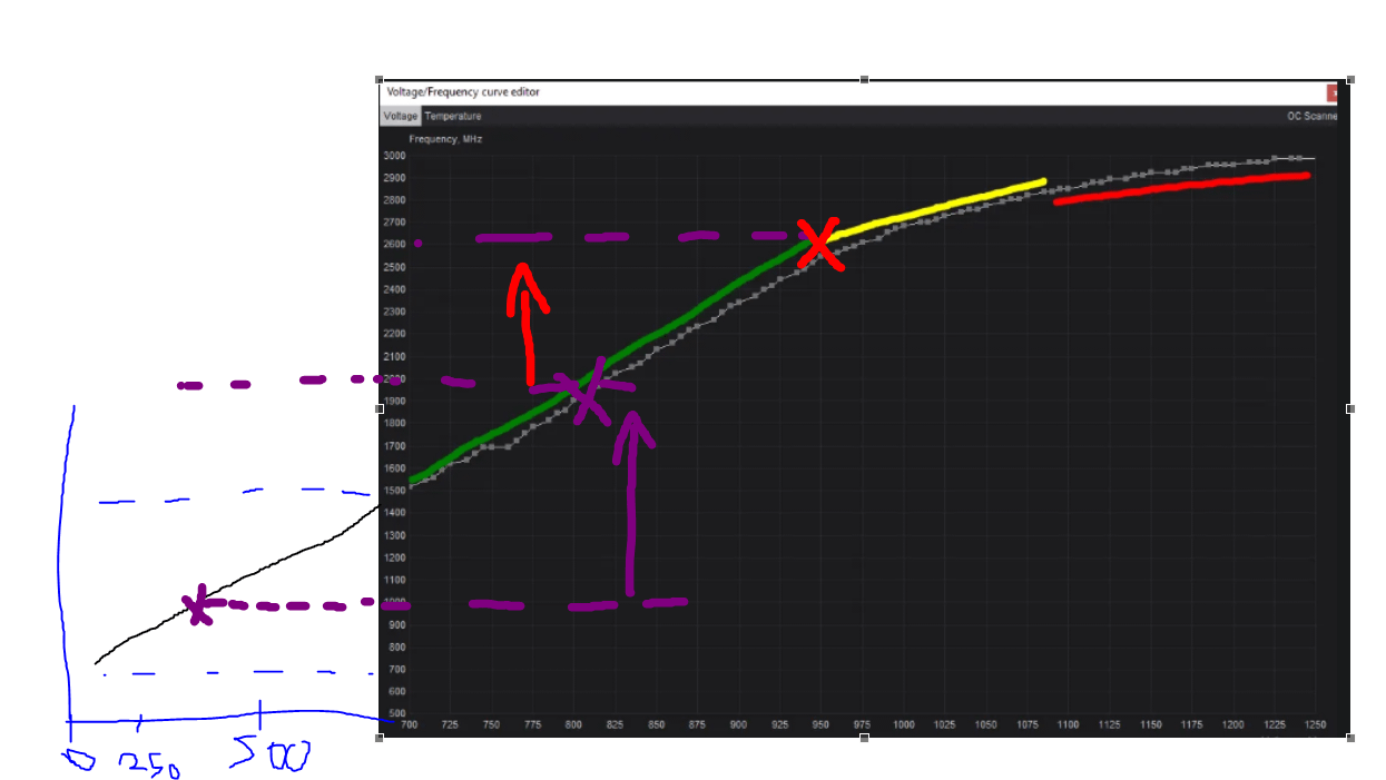
Ignore the absolute voltage and frequency numbers. I am using this chart because lazy.
Every chip has a volt/freq response that looks like this. Some threshold voltage to turn on at all, a linear region, a not so great region, then the asymptotic region where giving 20-25% more juice gives you 3-5% more speed.
I think Cerebras WSE3 and WSE3-turbo are at the purple Xs. The gain going from CS-3 to CS-4 is purple arrow. Red arrow and red X is where they would like to be but can’t for a variety of reasons where I can only speculate.
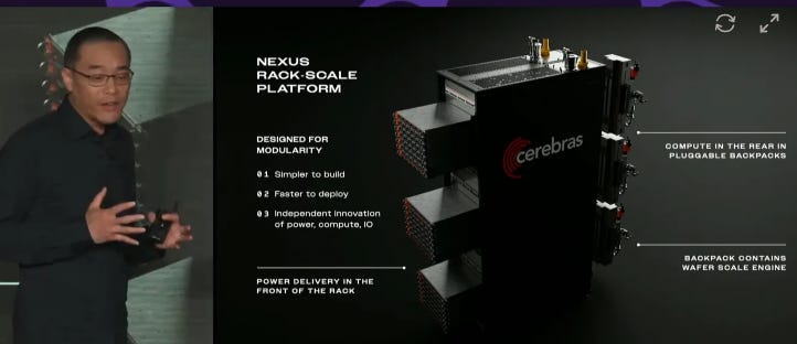
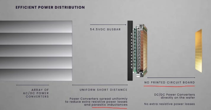
Note how JP called out resistive and inductive parasitics.
Parasitic resistance = power/efficiency loss
Parasitic inductance = power supply ripple = stability issues
Skewed corners (SF, FS) generally hate power supply ripple.
So on the enclosure, cooling, and power delivery fronts, Cerebras has made great progress.
I think the parametric (product-level) yield of this new system will be significantly better. They have supply issues now because this CS-4 product is only just starting to ramp. Probably have to wait until H1 2027 to see hardware revenue and gross margin inflection.
So the question is what can the next-gen WSE4 do to help with parametric yield?
Remember the WSE-3-turbo is the same silicon. Just doubled all clocks because of better thermal headroom and power supply stability.
Here is my list of ideas. All made up. I have no info just guesses based on experience.
Add granular voltage control by splitting up the power grids. The CS-4 renders look like the power delivery was modularized both for serviceability and for adjusting voltage of the WSE at a reticle or possibly more granular level.
Go a step further and add DVFS for the compute cores.
De-couple compute, SRAM, and NoC clocks.
New custom cells that are more tolerant to PVT. I suspect Cerebras used mostly standard PDK cells. Might be wrong on this.
As a summary // TLDR;
I believe Cerebras is getting killed by parametric yield issues which destroy hardware gross margins and severely limit supply.
Also believe CS-4 enclosure is great progress and should make their financials/numbers much better H1 2027.
There exist many possible vectors to drastically improve parametric yield further by making (admittedly significant) design changes in WSE4. Lot of potential here.