This project is a physical implementation of the Hack Computer, as described in the From Nand To Tetris course (nand2tetris.org). The course describes the hardware design of a simple computer and the software stack on top of it. I implemented the Hack CPU design and my own I/O controllers designs on breadboards using mostly 74-series ICs and wires that I cut and connected between the ICs.
Time-lapse:
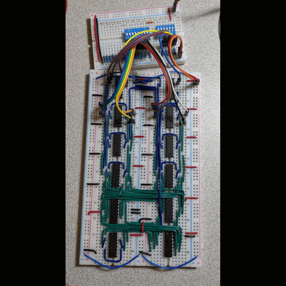
Table of contents:
- Summary
- CPU
- RAM
- VGA
- Keyboard
- Power Delivery
- Components
1. Summary
This project is a physical implementation of the Hack Computer, as described in the From Nand To Tetris course. The course describes the hardware design of a simple computer and the software stack on top of it. The computer described in nand2tetris makes some assumptions on the behavior of the Memory and I/O so I had to design and implement these components in a way that works with those hardware assumptions. I implemented the design on breadboards using mostly 74-series ICs and wires that I cut and connected between the ICs.
I took the nand2tetris course in my 4th year of my Electrical Engineering studies and during the course wondered if the Hack design can be physically implemented. I searched online and saw that the Hack computer was implemented on a FPGA, but I thought it would be so cool to see it running on actual chips and decided to go for it. I first thought about the idea of using only NAND gates, as we did at the actual course, but quickly understood it not feasible to do so. I decided on using ICs of basic logic elements like logic gates, MUXs, Adders and Counters.
Now, after about 2 years, I finished building the computer and it works perfectly. I had many challenges along the way, some with the design work and some with the implementation work. I needed to design the VGA and Keyboard controllers from scratch, and adjust the design of the CPU to work with a physical RAM chips. I also had bugs, so many bugs. Some bugs were design issues and oversights, and many of them were due to physical and analog phenomena that occurred on the breadboards. I had no idea when starting this project that I will need to invest that much time in fixing issues with signal noise, power delivery, reset and clocks. Also, the debug work got harder and harder the more components I added to the breadboard so I had to build tools for debug as well.
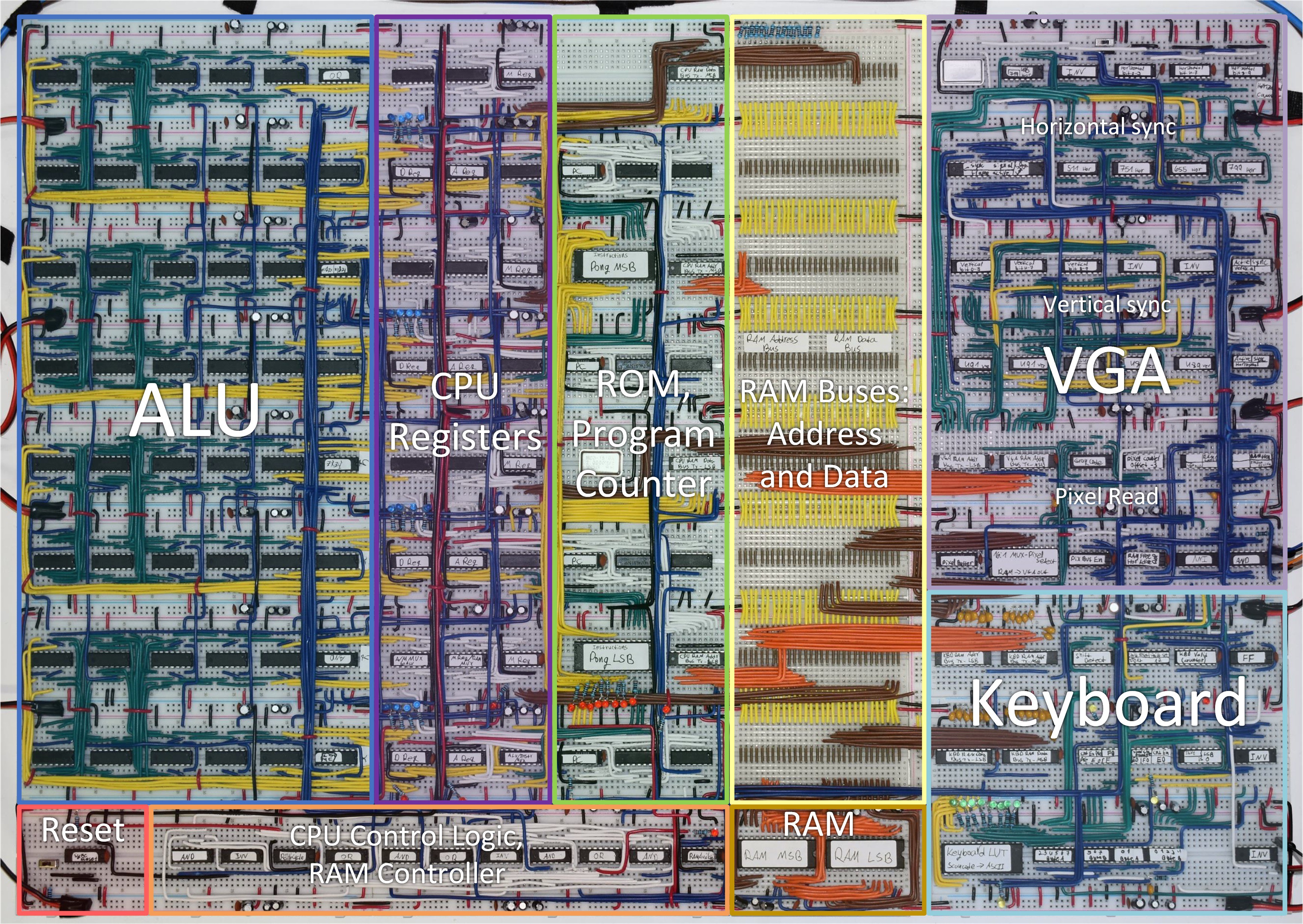
Here is a picture of the final layout of the computer with the functional description of each area.
Now, let's dive into the design and implementation :)
2. CPU
The CPU design is mostly identical to the described CPU in nand2tetris, aside from the addition of the "M Register" and some changes to the control logic. This changes are described in the following sections.
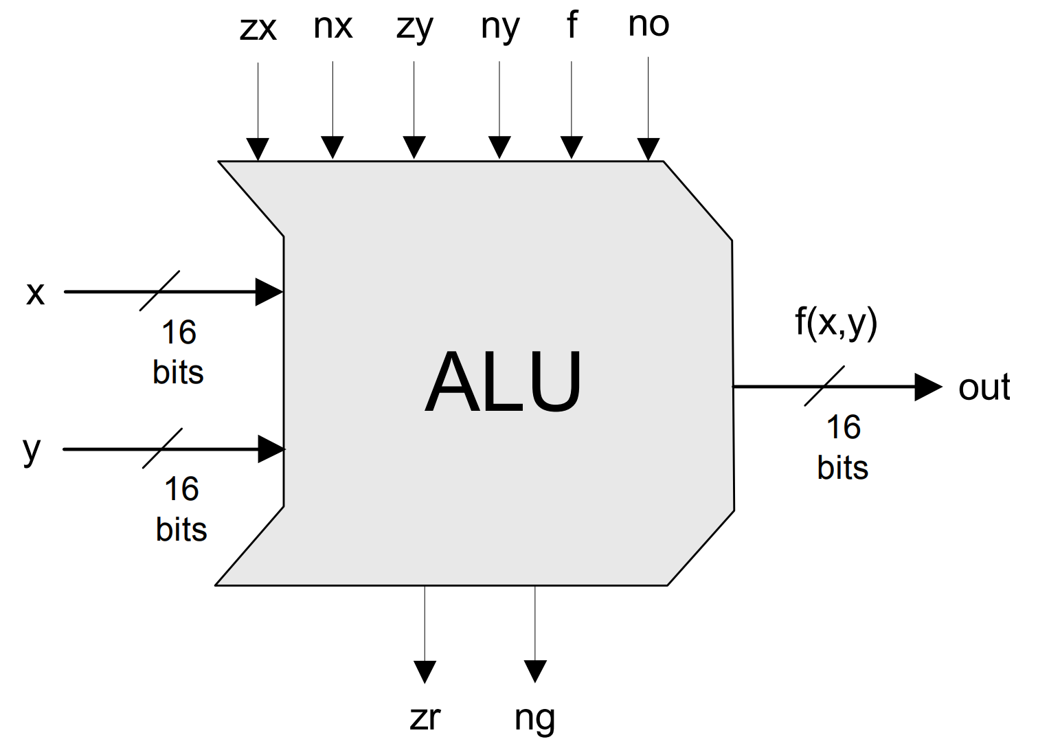
2.1 CPU: Arithmetic Logic Unit (ALU)
The ALU design is identical to what is described in nand2tetris, and is implements as follows:
- x3 = x2 + nx & zx ; x2 = ~zx & x1 ; x1 = x ^ nx
- y3 = y2 + ny & zy ; y2 = ~zy & y1 ; y1 = y ^ ny
- o1 = x3 + y3 ; o2 = x3 & y3 ; o3 = f ? o1 : o2
- out = o3 ^ no ; ng = out[15] ; zr = ~(| out)
This is the implementation that I found to require the least logic ICs on the breadboards.
The breadboard layout of the ALU is designed as 4 identical slices of 4-bits ICs: XOR, AND, OR, MUX 2:1 and 4-bit Full Adder. This was pretty repetitive to build, but very satisfying when finished :)
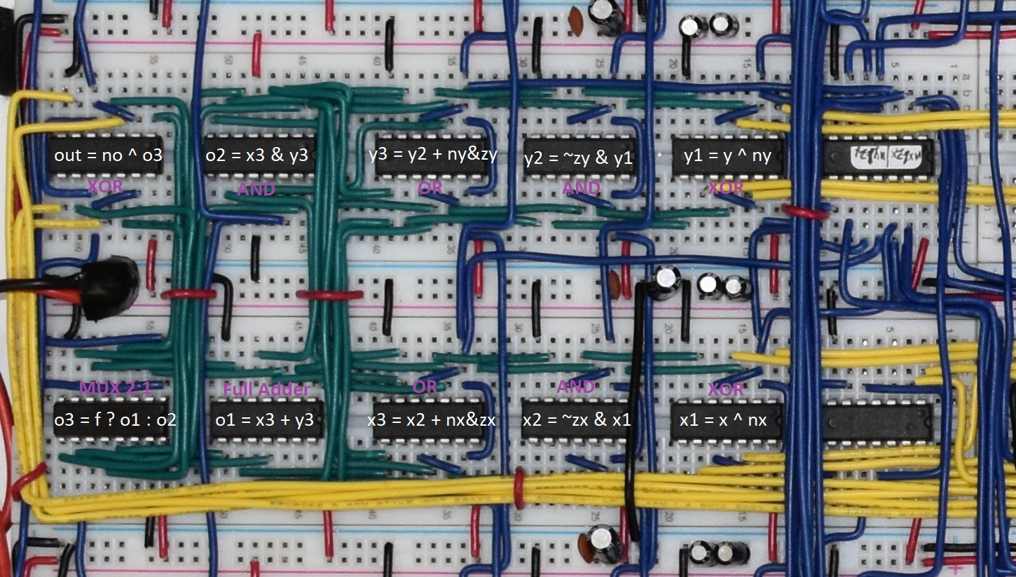
The 2 rightmost ICs in each of the 4 slices are for nx&zx, ny&zy and for calculating zr.
2.2 CPU: Registers (D/A/M)
The CPU registers and MUXs are as described in nand2tetris, except for the addition on the M register as shown in the diagram below. The M register is used to hold data that is read from RAM when executing an instruction that require both read and write from RAM (For example, M=M+1).
This was required as I chose to use RAM chips with a shared data bus for read/write...
scan_code_to_ascii_lut_publish.xlsxThe Look-Up-Table for the keyboard conversion on Scan Codes to ASCII characters sheet - 18.04 kB - 05/17/2022 at 11:10 |
Download |
- 8 × Logic IC 74LS04 Quad 1-input Not
- 36 × Logic IC 74LS08 Quad 2-input AND
- 19 × Logic IC 74LS32 Quad 2-input OR
- 13 × Logic IC 74LS86 Quad 2-input XOR
- 8 × Logic IC 74LS83 4-bit Full-Adder
Discussions
Become a Hackaday.io Member
Create an account to leave a comment. Already have an account? Log In.
![]()
Max wrote 01/01/2025 at 22:08
![]()
Tomer Kronik wrote 01/02/2025 at 17:03
Hi!
Sequential logic (flip-flop) allows to read the register's value, do the addition and the output the result to the register's input pin. Once the clock's positive edge arrives, the new value is stored in the register and the next cycle begins.
![]()
Max wrote 09/16/2024 at 13:56
Hi. Which IC did you use to convert the select signal of the 1:16 MUX on VGA signal generator, to gray code?

![]()
Aria wrote 07/06/2022 at 20:45
Very nice Kronik! I want to wire up something similar at some point. In the meantime I took the easier route and built it in Verilog for simulation then FPGA. I have the simulation up on my projects if you're interested: https://hackaday.io/projects/hacker/84292
![]()
eyal.a.porat wrote 06/05/2022 at 07:56
Absolutely great!!! Good job not giving up. I have seen a similar proj on YouTube by Ben Eater but you won him by the bits:). https://youtube.com/playlist?list=PLowKtXNTBypGqImE405J2565dvjafglHU
![]()
Are you able to do A=A+1 or D=D+1 in one cycle?
I don't understand how you can read and write, to and from, the same register at the same time without stuff going wrong.