TL;DR
I spent a few weeks sorting out some of the GEMM operations on Hopper and Blackwell using CuteDSL. I observed some of the evolution from Ampere to Hopper and then to Blackwell. Coincidentally, the weekend before last, I attended Huawei's Turing Computing Summit and had a chat with Dr. Liao and some other folks from the Ascend team. Following that, Jensen Huang's GTC keynote showcased the Vera Rubin engineering development board and BlueField-4, etc. Therefore, I am preparing to do a comprehensive analysis and a prediction of the next-generation microarchitecture (it's just a guess, so don't blame me if I'm wrong...).
In my humble opinion, Nvidia's biggest moat is not something that can be explained in a simple sentence or two. There is a lot of controversy around things like the CUDA ecosystem or SIMT. But its real moat is precisely the result of cleaning up a lot of the "dirty work" throughout the entire system architecture, coupled with a full-stack capability from algorithms to systems to chips. This is also a source of great inspiration for other chip manufacturers, especially in many subtle areas where the balance between ease of use/programmability and performance is well-managed. Another point is that the timing of the entire architecture's market launch and the marketing have been very well executed. As the saying goes, "One step ahead makes you a pioneer, but half a step ahead makes you a god."
Of course, every architecture has its trade-offs and shortcomings, and Nvidia is not a deity. I will also discuss many of Nvidia's issues, such as with Blackwell, Grace, and the newly released BlueField-4... Then, I will assume I am an architect for Vera Rubin and discuss what I would do to explore future evolutionary paths.
1. Discussing the Evolution from Volta to Blackwell
Since the introduction of Tensor Cores in Volta, Nvidia's traditionally defined SIMT architecture has already begun to be disrupted. The true completion of this entire architectural transition might not happen until the Rubin generation. This entire process has taken ten years, involving both gradual hardware iterations and progressive software innovations.
1.1 TensorCore
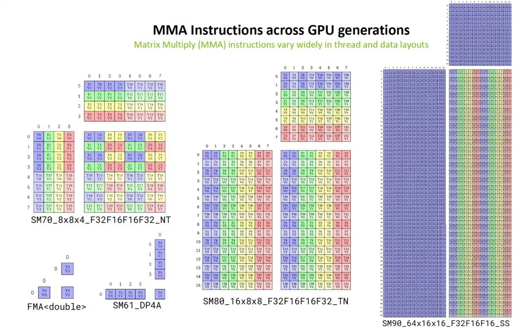
From a hardware perspective, starting from the earliest FMA instructions, to the vectorized DP4A, to the first-generation TensorCore in Volta (SM70), and then with Ampere/Hopper/Blackwell, the scale of matrix multiplication has been continuously increased, enhancing the compute-to-memory-access ratio while also supporting lower-precision data formats.
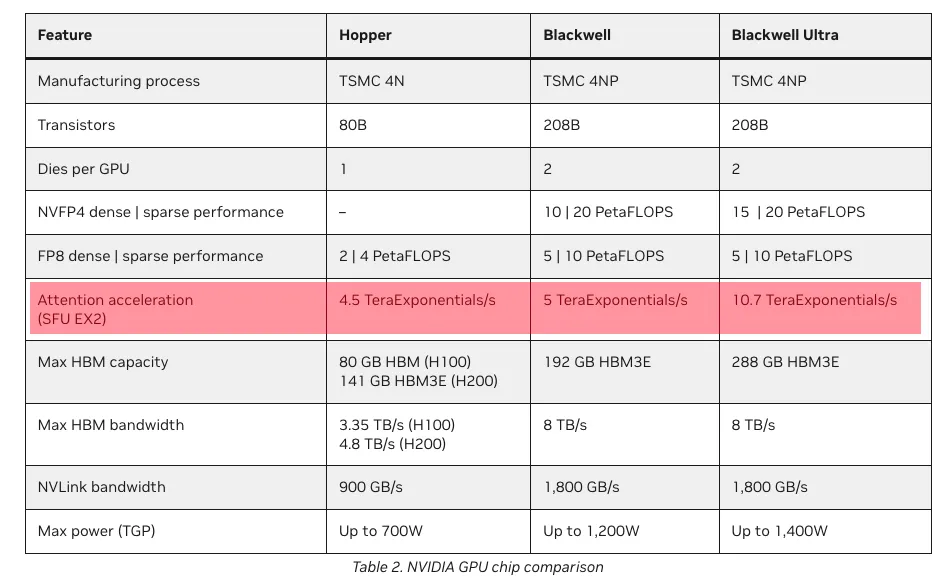
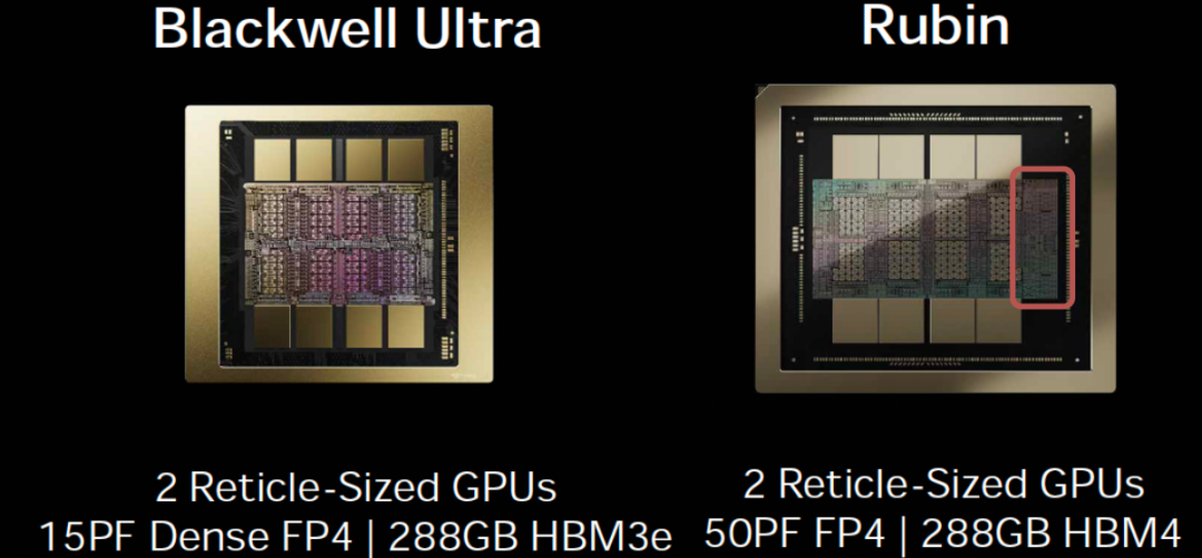
Looking at the changes in numerical precision, as shown below, constrained by chip area, the Blackwell Ultra (B300) generation has already started to cut back on the computational power for high-precision calculations.
| Arch | FP64 | FP16 | INT8 | INT4 | FP8 | MXFP |
|---|---|---|---|---|---|---|
| Volta | ❌ | ✅ FP16 | ❌ | ❌ | ❌ | ❌ |
| Turing | ❌ | ✅ FP16 | ✅ | ✅ | ❌ | ❌ |
| Ampere | ✅ | ✅ FP16/BF16 | ✅ | ✅ | ❌ | ❌ |
| Hopper | ✅ | ✅ FP16/BF16 | ✅ | ❌ | ❌ | |
| Blackwell | ✅ | ✅ FP16/BF16 | ✅ | ❌ | ✅ | ✅ MXFP(8/6/4) NVFP4 |
| Blackwell Ultra | ✅ FP16/BF16 | ❌ | ✅ | ✅ MXFP(8/6/4) NVFP4 |
It is expected that the Rubin generation will further double the scale of the TensorCore, likely to a size of 256 x N x 256 bits. On the other hand, I speculate that we will see an expansion from Blackwell's 2-CTA MMA to Rubin's 4-CTA collaborative MMA instructions. However, this will place further demands on scheduling within the CGA (CUDA Grid Array).
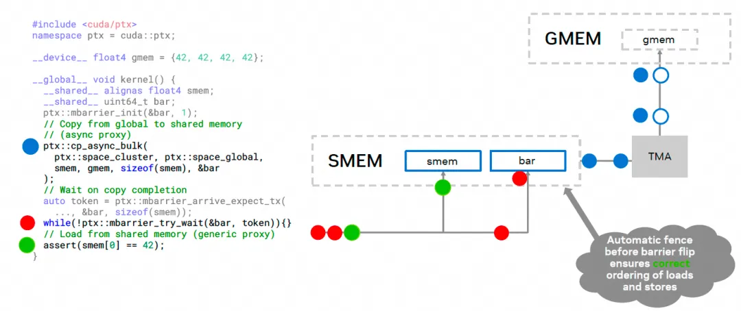
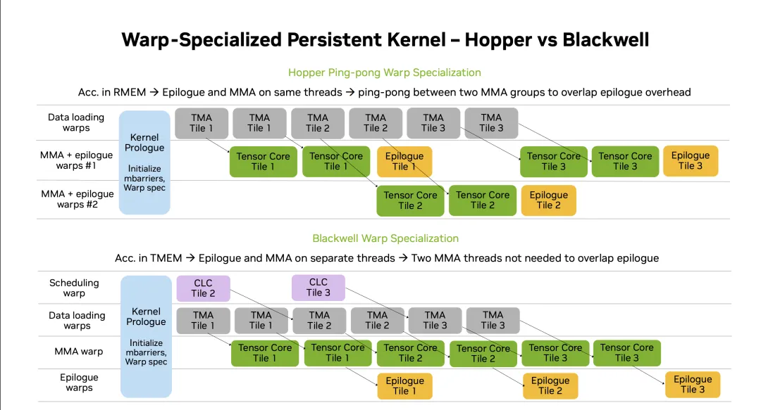
The increase in computational power also brings about changes in the data supply path. Early (Volta) TensorCores began by reusing CUDA Core registers. Then, as the scale of Ampere's TensorCores expanded, considering the pressure on the register file, cp.async was used to bypass L1 and reduce RMEM (Register Memory) occupancy. Moving to Hopper, TMA (Tensor Memory Accelerator) was introduced, allowing operands to be placed directly into SMEM (Shared Memory), and CGA and DSMEM (Distributed Shared Memory) were introduced. However, at this point, the accumulator results were still in RMEM to facilitate subsequent Epilogue operations, but this still required the use of a waitgroup barrier mechanism. Then, with Blackwell, TMEM (Tensor Memory) was introduced, essentially decoupling the TensorCore from the CUDA Core, and it also reused the Mbarrier mechanism introduced by TMA's asynchronous operations. This is shown in the figure below:
| Arch | Matrix A | Matrix B | Matrix D |
|---|---|---|---|
| Volta | RF | RF | RF |
| Ampere | RF | RF | RF |
| Hopper | RF/SMEM | SMEM | RF |
| Blackwell | TMEM/SMEM | SMEM | TMEM |
This entire process has taken nearly 10 years. Starting from Volta, where the TensorCore seemed like a temporarily added component, to Blackwell, which introduced TMEM for a nearly complete asynchronous separation independent of RMEM, each step has been taken very steadily.
For more details, you can refer to the following two special topics:
《History of GPU Architecture Evolution》
1.2 Asynchronous Processing
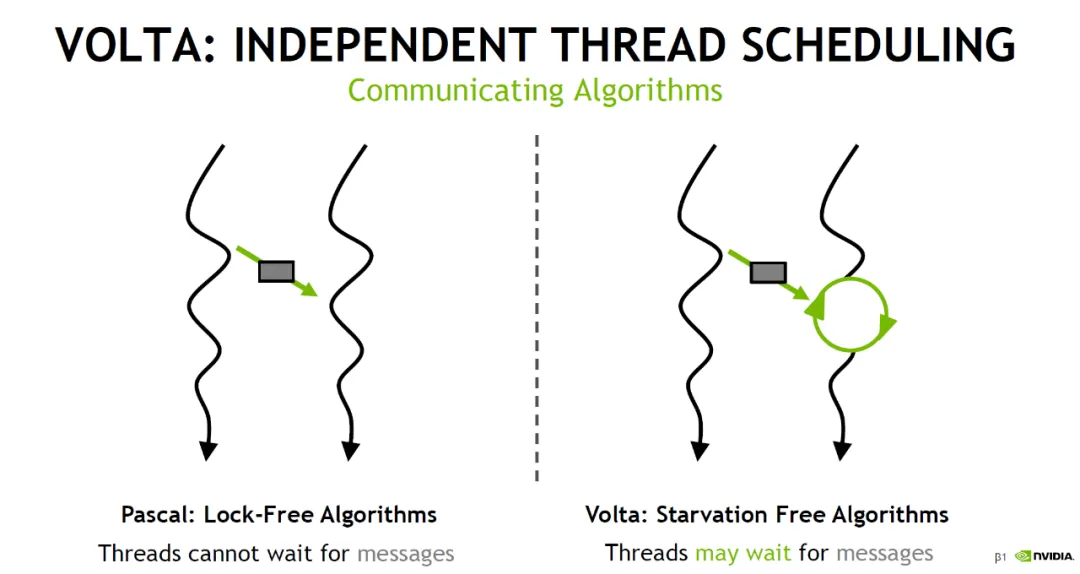
Another aspect is the move towards asynchronicity. When Volta introduced an independent Program Counter (PC) for each thread, it actually marked the beginning of this asynchronous trend.
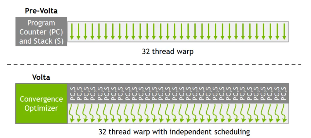
With this, threads could start waiting for certain messages to perform asynchronous processing, which opened a window for asynchronous programming compared to traditional architectures with aligned PCs.
A good thing is that Nvidia provided the Cooperative Groups abstraction in software. However, TensorCore operations still needed to be executed synchronously across the entire warp. Then, starting with cp.async in Ampere, the program's data supply path effectively became asynchronous, which is what Nvidia refers to as the "Async Thread" concept.
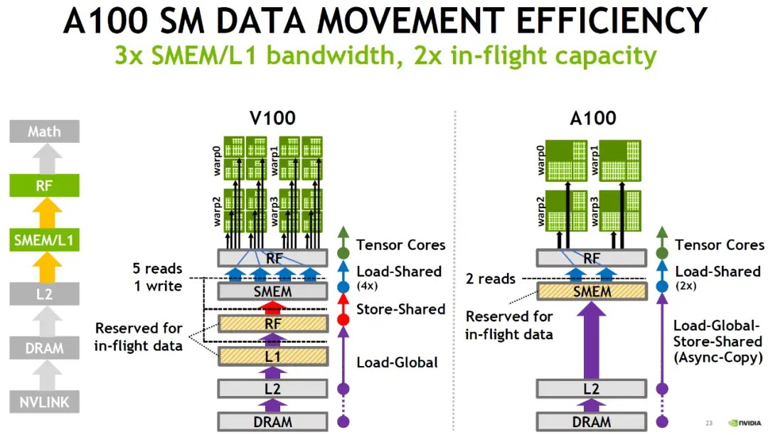
Hopper went a step further by introducing MBarrier. In software, asynchronous pipelines built around MBarrier and Warp Specialization became popular. It also introduced the Async Proxy, distinguishing different memory access paths through the General Proxy and Async Proxy. For Async Proxy operations, there is usually a memory barrier. General proxy LD/ST operations can wait for this barrier to complete, allowing TMA and other asynchronous operations to be integrated with the original SIMT memory access LD/ST instructions, ensuring memory ordering requirements.
Of course, Hopper also had its imperfections. WGMMA was a temporary solution that occupied a large amount of RMEM and required synchronous waiting. Therefore, at the time of Hopper's release, it was explicitly stated that SM_90a's WGMMA would not be backward compatible. This has a major drawback:
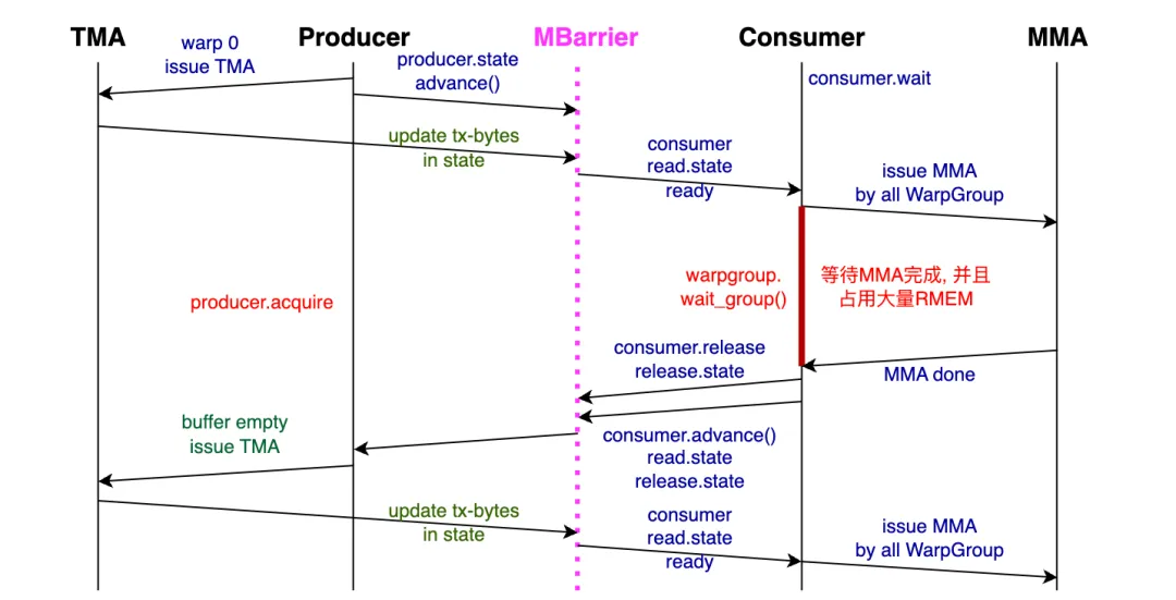
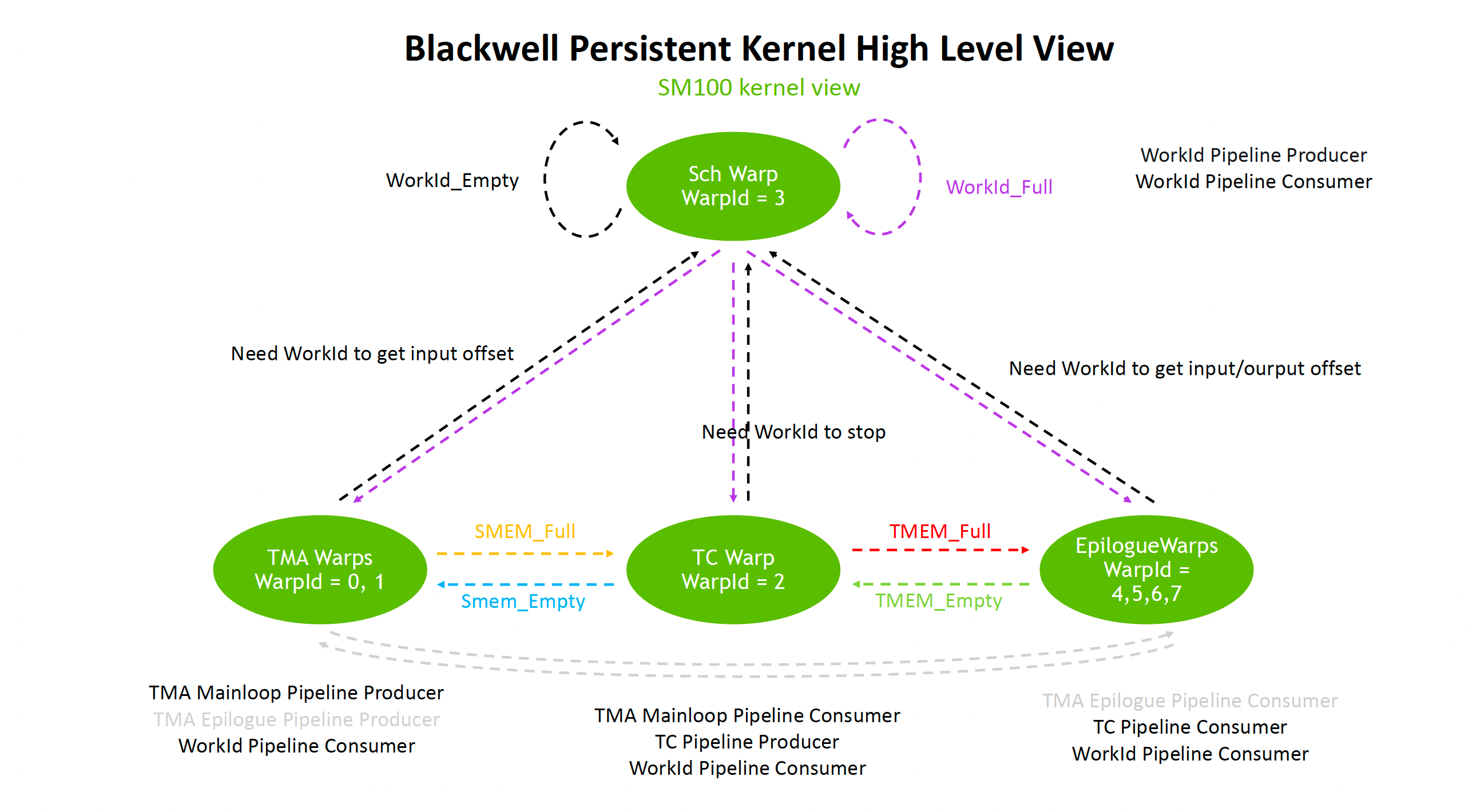
With Blackwell, TensorCore operations also became fully asynchronous and reused the MBarrier mechanism. Therefore, issuing TMA and tcgen05.mma instructions can be done at the thread level. However, memory allocation and copying for TMEM still require Warp-Level handling. Another point is the introduction of the ClusterLaunchControl mechanism, which provides some capability for dynamic scheduling.
Then we can build more complex Warp Specialization processing models.
For more details, you can refer to:
《Discussing GPU Memory Models and Interconnect Network Design》
1.3 CuTe Layout
This is also an excellent software abstraction, especially on Hopper and Blackwell where it hides the complexity of swizzling. On the other hand, from an algebraic perspective, it solves complex tile/partition boundary calculations, making the code more intuitive. Of course, for those not specializing in algebra, learning CuTe still presents a steep learning curve. I have started a discussion on CuTe Layout algebra below:
《CuTe Layout Algebra - 1: Overview》
But you need to be aware that in the Blackwell dual-die architecture, or even the Rubin Ultra 4-die architecture, and future 3D-DRAM architectures, this set of algebra has already simplified many problems. I will elaborate on why in the following chapters.
Of course, I will continue to update this content in the coming months as I have time.
2. Discussing Blackwell's Shortcomings
Having said some good things, this chapter will discuss some shortcomings, mainly for the purpose of demystification.
2.1 The B200 SFU Problem
In the frantic race to boost TensorCore performance, a large amount of TMEM was added. At the same time, the DSMEM formed by some interconnect networks within the GPC also took up a lot of die area. The removal of L2 partitions also consumes die area. As a result, the number of SMs on a single die was reduced to 80. Unfortunately, the performance of the SFU (Special Function Unit) paired with the CUDA Cores was not enhanced. This leads to what seems like much stronger GEMM performance but creates a bottleneck when calculating Softmax in Attention.
Of course, some people might say, "What's the problem? We can just use Linear Attention." Indeed, recent changes in Attention have brought some controversy. On one hand, there are Qwen-Next's GDN and Kimi Linear's KDA. On the other hand, Minmax M2 has abandoned Linear Attention. Another path is seen in Google/DeepMind's MoR and the rumored Universal Transformer in GPT-5, which seem to be further strengthening the computational power of the Attention block.
《Discussing Some Evolutions of the Transformer: UT, MoD, MoR...》
And DeepSeek-V3.2's DSA and the previous NSA are heading down the path of Sparse Attention.
My personal view aligns with DeepSeek's: Linear Attention does not solve the memory access bottleneck well. Computation itself is easy to scale, but memory access is very difficult. Therefore, choosing Sparse Attention is the right path.
Another point comes from an article I read some time ago, which views SDPA from the perspective of optimal transport. It states that the forward pass of the attention mechanism, specifically the process of generating attention weights via the Softmax function, is perfectly equivalent to the exact solution of a One-Sided Entropic Optimal Transport (EOT) problem. Therefore, Softmax is unavoidable.
Based on this perspective, my personal view is that the capability of the SFU must match the computational power of the TensorCore. Fortunately, this problem is solved on the B300, at the cost of cutting a lot of other high-precision computing power. Regarding this issue, I have always felt that the B200 and GB200 are not very worthwhile investment platforms.
2.2 Blackwell's Complex Instruction Structure
The truth is, starting from Hopper, asynchronous programming had already become very complex, and Blackwell's introduction of TMEM has actually added more complexity. For example, the entire TensorCore tcgen05 instruction has both synchronous and asynchronous forms.
tcgen05.* operation |
|
|---|---|
| Synchronous Instructions | .alloc .dealloc .relinquish_alloc_permit .fence::* .wait::* .commit |
| Asynchronous Instructions | .mma .cp .shift .ld .st |
On the other hand, the granularity of issued instructions is also different; some are thread-level, while others are warp-level, and one also needs to consider the 2-SM case.
[Image: A table or diagram showing the different granularities (Thread, Warp, 2SM) for various instruction types, highlighting the complexity.]
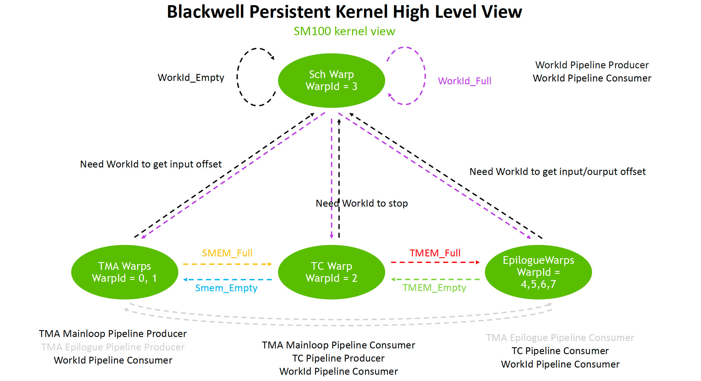
It's easy to make mistakes if synchronization is not handled properly. However, Nvidia has introduced many pipeline abstractions here, which helps avoid many errors. Paired with TMEM's memory management and allocation mechanism, the complexity of managing TMEM in a multi-threaded parallel context is reduced through alloc/dealloc.
In fact, from a management complexity perspective, the Sch warp, TMA warp, and TC warp in the diagram below can all be handled at the single-thread level. Only the EpilogueWarp needs the old SIMT-style approach. Once you understand this, it doesn't seem that complicated.
2.3 CPU Problems
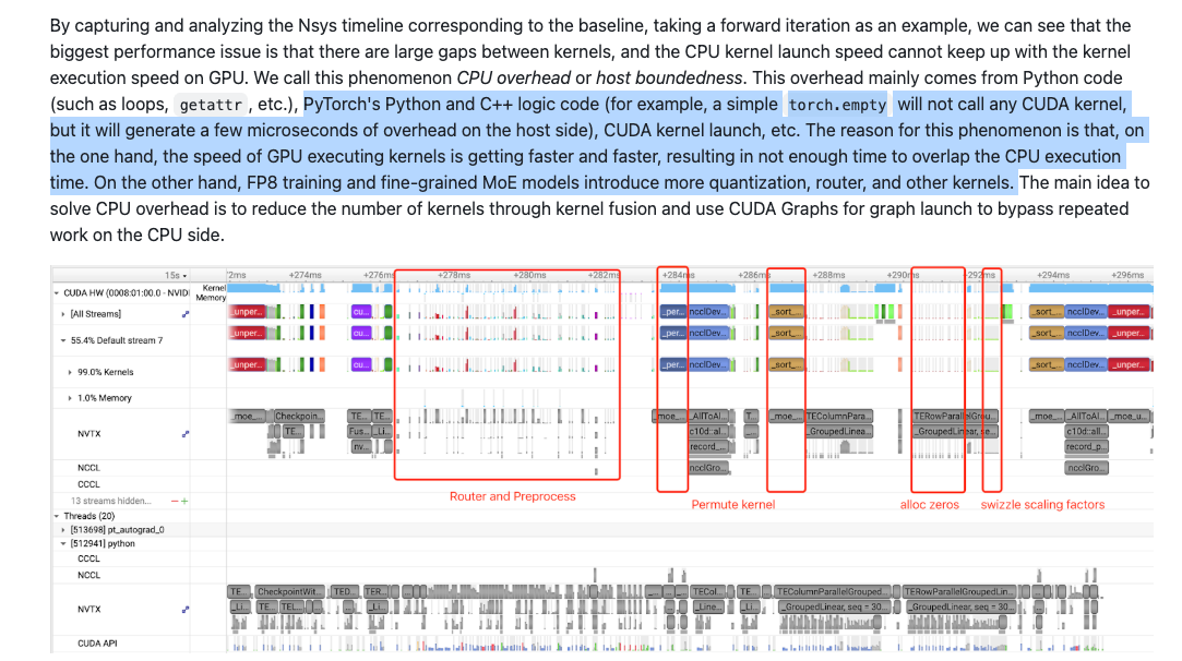
Although NVLink C2C was introduced in the Hopper generation, allowing Grace to connect directly to Hopper or Blackwell via NVLink, the Grace CPU itself has quite a few problems. As Blackwell's computational power grows stronger, the execution time of many kernels has dropped to the microsecond level, which creates the classic "Killer Microsecond" problem. For nanosecond-level issues, synchronous waiting is fine. For millisecond-level times, the cost of context switching is not significant. But when it comes to the microsecond level, it's actually a big challenge for the processor. Although many asynchronous programming optimizations have been introduced, CPUs like Grace still face many bottlenecks. One is that the kernel launch speed is not fast enough. While one can argue this can be solved with CUDA Graphs or some persistent kernel methods, not all workloads fit this condition.
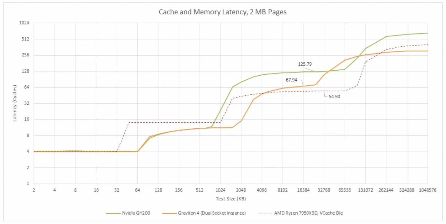
Another issue is some of the microarchitectural flaws of Grace. Although Grace uses ARM's then-most-powerful Neoverse V2 core, its design did not adopt the 2MB L2 cache used by V2, but rather cut it down to 1MB. In contrast, AWS's Graviton 4, which also uses the V2 core, employs a 2MB L2 cache. Some customers are currently encountering significant L1 ICache Miss problems on the GB200, which is largely related to this. We can see that in Nvidia's promotion of Grace, they basically only talk about HPC-related applications...
Another emphasized point is the balance between larger memory bandwidth and capacity, for which LPDDR5x was chosen, further expanding the memory access capability of Hopper and Blackwell through NVLink C2C.
Then, the on-chip network is also a Mesh architecture, and the access latency for the entire L3 cache requires multiple hops on the NOC, which also has a significant impact.
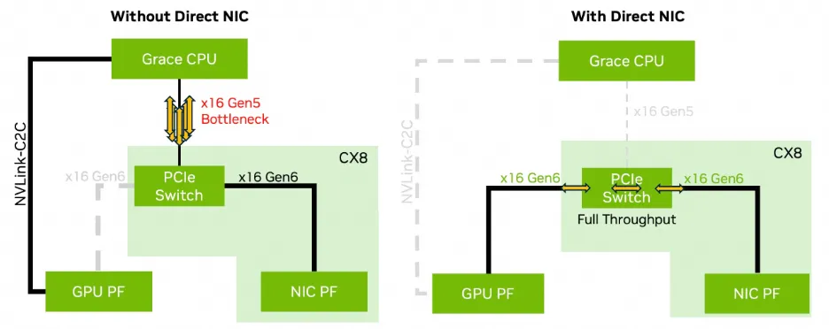
Furthermore, with the GB200, the paired CX7 does not have a built-in PCIe Switch, so ScaleOut RDMA traffic will traverse the entire Grace NOC and then pass through NVLink C2C to reach Blackwell.
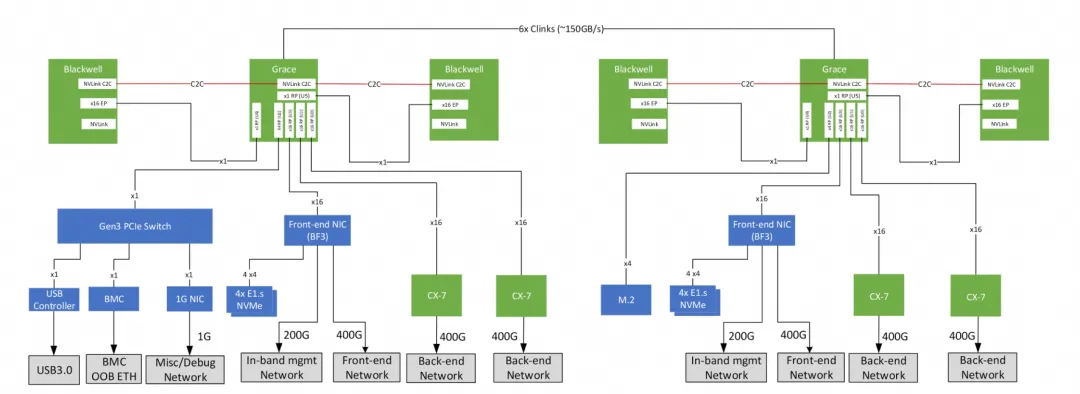
This can cause quite a few problems. For example, when this traffic traverses the entire Grace NOC, in a situation with a smaller L2 Cache, the penalty for a cache miss will be further increased. There is a test on Chips and Cheese showing that Grace's latency is much higher than X86, and also significantly higher than Graviton 4, due to the L2 cache being too small and the significant impact of noisy neighbors and NOC noise.
By the way, a little rant: The Grace-based BlueField-4 has the same problem... NV's capability in this area is really not good. On another note, there are major design problems with the CX8/CX9...
In fact, if we look at a recent Megatron report on training DeepSeek-V3 on GB200, 《Optimizing DeepSeek-V3 Training Performance on NVIDIA GB200 NVL72》, it also mentions this CPU overhead problem.
AWS addressed the issue of ScaleOut RDMA traversing the Grace NOC by adding an external PCIe Switch.
Meanwhile, Meta mitigated it by changing the ratio of Grace to Blackwell to 1:1.
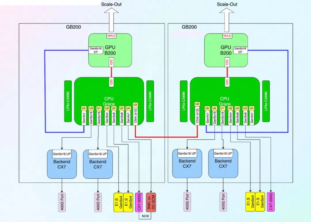
Of course, some of these problems are solved in the GB300.
In contrast, let's look at Intel's GNR (Granite Rapids). It has SNC3 (Sub-NUMA Clustering) options for cache handling:
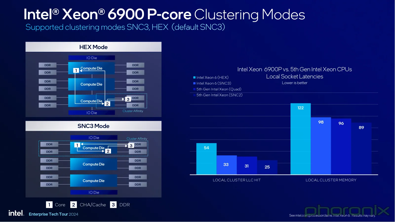
Of course, GNR also has some NOC-related issues that affect memory speed, but I won't go into detail... The essential problem is that once the number of cores reaches a certain level, the complexity and performance impact of the NOC become very significant, especially for these general-purpose CPUs with cache coherency. Even for non-cache-coherent processors, for example, when I was at Cisco, the first-generation QFP with 40 cores and 160 threads in 2004, and the second-generation with 56 cores and 224 threads in 2008, were both fine. But when we expanded to the third-generation QFP3 with 224 cores and 896 threads, we encountered a large number of problems. In reality, once a single-socket general-purpose processor scales to several hundred cores, it will encounter similar issues... I won't go into the specific details...
2.4 Blackwell Memory
Another issue is the dual-die architecture. Cross-die memory access will inevitably bring greater latency. This will cause problems with the efficiency of SMs accessing GMEM. Currently, CUDA 13.0 does not support CTA memory affinity scheduling, but my intuition is that some things can be done through CuTe Layout to stagger memory banks. Of course, whether CUDA will add similar CTA affinity scheduling APIs in the future, I estimate it will... I wrote an article about this before:
《Nvidia GB200 Architecture Analysis 4: Analysis of Blackwell's Multi-die and Cache Coherency》
3. Predicting Vera Rubin's Architecture
3.1 Vera CPU
Judging from the development board Jensen Huang showed at GTC, first, Vera's memory uses 8 channels, so the memory bandwidth should be double that of Grace. The number of CPU cores has increased to 88, and it will likely support 80 lanes of PCIe Gen6. The core spec is probably ARM's Neoverse V3. V3 can support up to a 3MB L2 cache, but I'm not really sure how NV will choose. At least the Neoverse V3-AE introduced in Jetson Thor is still stuck at a 1MB L2 cache... Also, it is a multi-die structure, placing the PCIe/Memory Controller on a different die, a design consistent with Graviton 3/4.
However, the CPU overhead will likely still exist. The fundamental reason is as follows: it usually takes only 3 cycles for a CPU core to read from L1 cache, but when it needs to traverse L3 and faces a Mesh NOC, it usually takes 120 cycles or more.
Of course, this problem is not that big. Perhaps it will be alleviated when an Intel x86 CPU with NVLink C2C appears...
3.2 Rubin Architecture Speculation
There are already some things that are public knowledge, for example, the scale of the TensorCore will be further expanded by a factor of two in the M dimension, and the capacity of TMEM will likely increase to cope with this change. But the entire chip area is already stretched to its limit. It is precisely this area constraint that has led Nvidia to adopt a separate I/O die for Rubin.
Then, I speculate that locally, a 4-SM MMA will be used to further reuse data. The CGA cluster shape will go up to 4, and it will continue to use Blackwell's preference cluster shape method to schedule and fully utilize the entire GPC.
Regarding the SM microarchitecture, based on some observations from Blackwell, I think adding a scalar core within the SM could yield many benefits. The entire scalar core plus a private SMEM would take up very little die area.
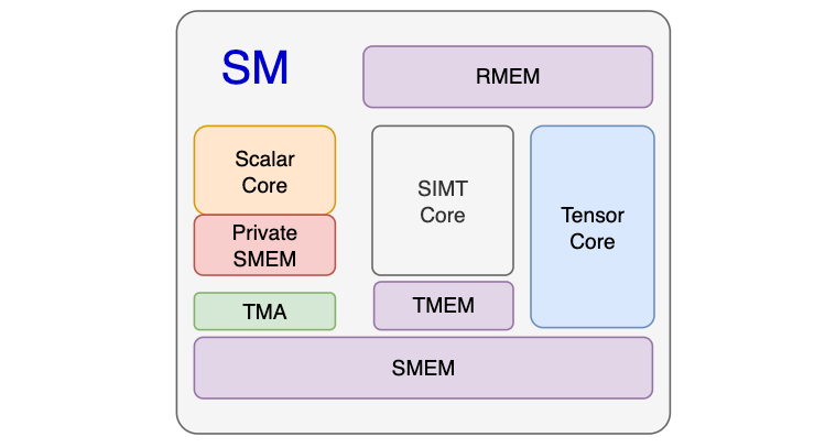
First, TMA/MMA descriptors are now basically generated by the host CPU. Although there is NVLink C2C between the host CPU and Rubin, the latency is still very high. Another reason is that issuing TMA and UMMA and scheduling the cluster only requires a single thread, so there is no need to run it on a CUDA Core.
Then, I would design a small piece of private SMEM (e.g., 2KB~4KB) for it to store MBarriers. This way, the asynchronous program architecture can be more easily decoupled, without needing complex Warp Specialization handling. It would just be a TC Function, a TMA Function, and the original CUDA SIMT kernel function for the Epilogue. Then, functions related to scheduling warps and preparing TMA/TC descriptors would be placed on this scalar core. It could even be taken a step further to interact more deeply with the Warp Scheduler. In essence, it's similar to the ideas in Halide/TVM/Tae-lang, using a method that separates scheduling and algorithm.
Additionally, for things like GIDS (GPU Initial Direct Storage), some file system processing logic could also be placed in this scalar core.
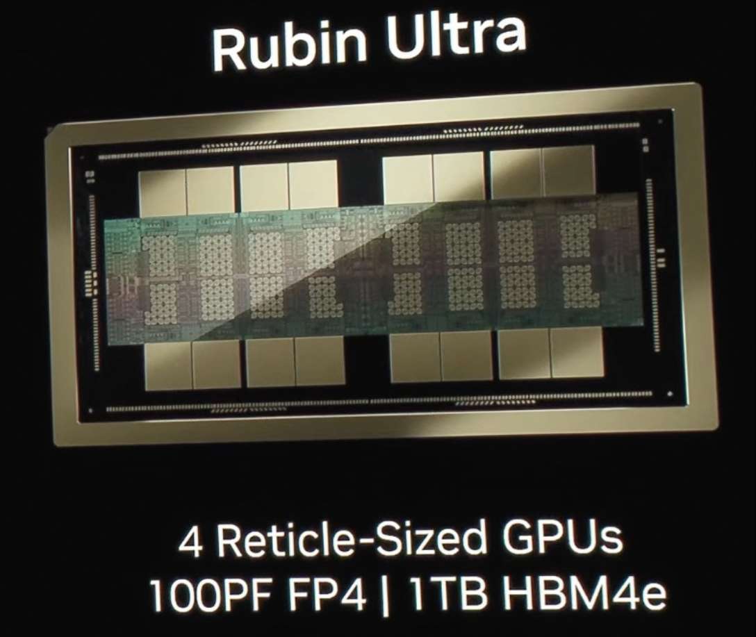
In this scenario, we could even do some more complex MPMD (Multiple Program, Multiple Data) programming and experimentation. Especially on Rubin Ultra, with 4 dies stitched together, there are many interesting parallel strategies that can be implemented.
For example, using something like Green CTX in combination with CTA affinity to better utilize the on-chip structures. In fact, MPMD frameworks like Google Pathways have been around for a long time.
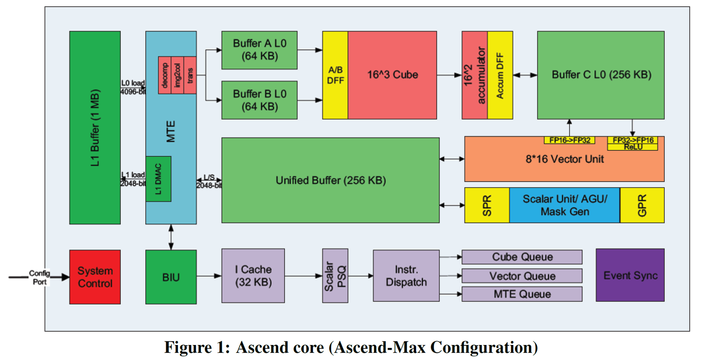
Then you might say, "Hey, isn't this very similar to Huawei's Ascend 910? It also has a scalar AI CPU, a SIMD Vector Core, and a Tensor Core."
This is what I was alluding to earlier with "one step ahead makes you a pioneer, half a step ahead makes you a god." A large part of Nvidia's success lies in its slow guidance of the entire computing ecosystem, letting customers start with Volta's TensorCores and slowly reach this point over a whole decade. People in technology easily fall into building things with an "end-state-first" mindset. I've made many similar mistakes myself, for example, when I was working on AI Infra at Cisco in 2018, implementing dynamic control algorithms with neural networks on Cisco's network devices, and developing edge AI-related hardware products. It's only now that Cisco is releasing edge AI products... these are all things I had completely finished 8 years ago...
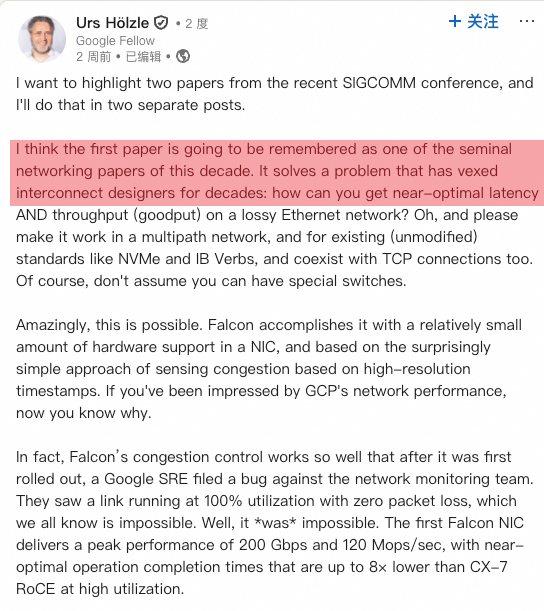
When the world's collective understanding is at a certain point, many things that are too far ahead will end up like Giordano Bruno, burned at the stake... For example, to change the topic, RDMA's Lossy vs. Lossless... when the whole world is on Lossless, being too far ahead can also cause problems. It's only now that you have to consider scaling across... Look at what a Google Fellow says; he said Falcon is a very important paper from the last decade.
And our eRDMA was like that 3 years ago...
《Discussing Google Falcon's Reliable Transport Paper and a Comparative Analysis with CIPU eRDMA》
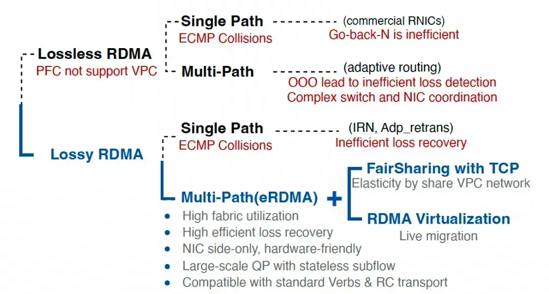
The diagram below is the right way forward.
However, after being beaten up by the market, I've learned my lesson. Many times, even if you see things clearly, you have to follow the market's rhythm and evolve slowly according to user mindset and the ecosystem.
Returning to the main topic, there are actually many subtle differences in GPU microarchitecture, such as the controversies between SIMD vs. SIMT, task scheduling frameworks, memory barrier design, scalar core architecture, on-chip NOC interconnects, etc... A more important issue is the balance between ease of use and performance. An architect needs to ensure that customers do not fall into a performance-collapsing case due to programming difficulties.
There is a huge amount of dirty work here. On one hand, you need to have a deep enough understanding of the algorithms running on top of it. For example, as mentioned earlier, viewing SDPA's Softmax as an optimal solution from the perspective of Optimal Transport. Then, from a computational efficiency standpoint, memory is hard to scale, so you wouldn't choose the Linear Attention route, but rather lean more towards Sparse Attention. Once you understand this principle, you won't go cutting SFU compute power. It was rare for Nvidia to make a mistake on the B200, but fortunately, they saved it with the B300.
As a chip architect, you mostly have to predict the workloads of the next 3-5 years. Of course, this is difficult, but Nvidia has full-stack capabilities, and that is their moat. We, on the other hand, might have to rely on "human" intelligence.
Also, a prediction from six months ago:
《Predicting the Architecture of Large Models for the Next Five Years?》
Of course, the cost of being "human-powered" is very high. After spending nearly twenty years going in circles, I have gained a lot from covering almost everything from algorithms to chips. From the chip perspective, having worked from networking to computing, in the interconnect area, whether it's protocol design or chip implementation, we are very much ahead. I still remember a few years ago when NV came to talk to us about the BlueField-4 roadmap, we had already implemented their RDMA-related roadmap items. The next-generation chip will have no problem crushing the CX10, so everyone can rest assured.
For Scale-UP, you basically can't find many experts in the world who know more than I do; all the trade-offs have long been analyzed.
《Discussing RDMA and Scale-UP Reliable Transport》
In the area of operators, I have basically filled the gaps very quickly recently. Although I started writing CUDA many years ago, I recently bought a Jetson Thor and have completely figured out Blackwell's microarchitecture and programming. What might be lacking is some framework-level code, which I should be able to catch up on by training a smaller model next month without much issue.
As for algorithms, from my early days in competitive programming (OI) to quantitative algorithms, to training my own models at Cisco for distributed reinforcement learning-related optimal control, and using graph algorithms to analyze device anomalies and accelerate distributed database searches, I've been doing that for many years. As for mathematics, perhaps I'm not too bad, after all, I spent several years in the math department taking dozens of math courses. I basically saw things clearly by 2014, although I am still working hard on learning algebra...
《Mathematical Foundations in the Era of Large Models》
4. Some Advice
Two weeks ago, at Huawei's Turing Technology Summit, I also talked about this with Dr. Liao and some folks from the Ascend team.
Many times, the devil is in the details. For example, how are Nvidia's SM interconnects, especially within the CGA, implemented? Why was MBarrier designed that way? How is the Async Proxy designed? What help does it provide for simplifying asynchronous memory access in software? How are these complexities wrapped in software abstractions? Why is CuTe Layout abstracted in that way? Even in the small details of usability, for example, a very small detail in tcgen05: why do they wrap tcgen05.commit inside pipeline.consumer.release, and why did they implement column-based alloc/dealloc on TMEM? Of course, once you understand the design itself, it's very simple, but there are many trade-offs involved behind it. The point of usability is not just a simple ecosystem problem; it's more about understanding not just the "what" but also the "why."
There are no shortcuts for these things; you must do every detail well, step by step. So-called "corner-cutting to overtake" will most likely lead to "crashing on the corner"...