Disclaimer: Opinions shared in this, and all my posts are mine, and mine alone. They do not reflect the views of my employer(s), and are not investment advice.
Hello there. If you are reading this, we have probably already interacted in the past. I was created a long time ago, inspired by a project management tool called Program Evaluation and Review Technique (PERT), that was used to identify the critical path and slack time in projects. I still carry some of these terms with me - from 1966 all the way till today. You may know me today by different names like Synopsys PrimeTime, or Cadence Tempus - does that ring a bell? No? It’s okay, I know I am not as popular as those pretentious synthesis tools that bully me around. But I play an important role in your life, and I’m here to tell you why…
As you may have guessed, what I do is called “Static Timing Analysis”. The cool kids call it STA, so let’s stick to that. You know how you use a modern hardware description language like Verilog to describe your digital design? Well those languages might make your life easy, but tools like me can’t comprehend all the fancy slang you use there. Am I supposed to know what “always @ posedge” means? No thank you. All I understand are the basics:
What are the inputs and outputs (Called “IO”)
Simple logic components, like gates (AND, OR, etc.) and MUXes (Called “Cells”)
Storage elements like Flip-Flops, Latches (Called “Registers”) and SRAMs (Called “Memories”)
Connections between them (called “Nets”)
So before you come asking for my help, you need to convert your fancy HDL design into something I understand called a “Netlist”. (A list of nets, get it?) That’s where the synthesis tools come in - they are just fancy translators who understand your HDL design, and break it down into the simple netlist that I understand. They don’t check whether it is even possible to have the connections you have described - they just want to please you by saying yes to everything you say. No wonder you like them so much.
But let me tell you the harsh truth - not everything you describe is realistic. You might think you are the god of chip design, but in my world, you must bow down to our god - Physics. What you are designing is not software - a chip is a physical entity that works by moving electrons. They’re much faster than anything you’ve ever seen, but they still take time to move from one place to another in the chip. Due to this fact, any logic you add in the chip will also add a delay. Your favorite synthesis tool conveniently left all this out.
Finding out exactly what this delay would be is challenging - remember, at this stage, I am doing this with no knowledge about how the chip is going to look at the very end. But even at this stage, I have something valuable that no one else has - estimated delays of different cells for the technology that the chip would be manufactured in. (In other words, a direct line to Dr. Morris Chang - ever heard of him?) I write down this information in a place called the “Cell Library” - I’m going to need to refer to this often once I get started with my work. But I still haven’t told you what my work is, have I? Before I do that, I will tell you why my job exists in the first place.
Now that you know delays are a thing in the real world, let me introduce you to the idea of synchronization in digital design. Consider this design I once worked on, where there were 5 inputs - A, B, C, D, and E, used to get the final output O. When I saw the netlist, I noticed that this design includes an AND gate, two OR gates, and a MUX, connected like this:
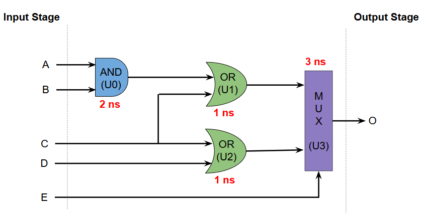
As you can see, I have also added the delays of each cell by checking the cell library. (You’re welcome.) Assuming no input delays, the time taken to observe the correct output O can be obtained by adding all the delays in the path between an input and the output. However, there are multiple different paths from the input and output, each with a different delay:
Path 1: Input A/B → U0 → U1 → U3 → Output O (Delay = 6 ns)
Path 2: Input C → U1 → U3 → Output O (Delay = 4 ns)
Path 3: Input C/D → U2 → U3 → Output O (Delay = 4 ns)
Path 4: Input E → U3 → Output O (Delay = 3 ns)
The purpose of any digital design, is to find the output when the input changes. Since the delays are different, you don’t exactly know when the output is ready - it could be 3 ns, or 6 ns after the inputs are applied. This makes the design pretty much useless. How do we deal with this problem? In the above example, let’s say that the input can only change once every 10 ns, and the output is also sampled with the same frequency - then, irrespective of the path between input and output, we are guaranteed to get the correct output value. In other words, by restricting when inputs to a design can change, and outputs from a design are sampled, we can ensure correct execution across many different paths - an idea called synchronization.
In order to maintain synchronization, we need to ensure that the input remains unchanged. But we have no idea where these inputs are coming from, so each input may have it’s own delays. This means we need to have a way to store the values of the inputs periodically, and use these stored values to calculate the output. This is done using a storage element like a latch or flip-flop - the general term for this is a Register. Let’s add registers R0 and R1 at the input and output of our design, respectively.

Each register also needs to know when to store the next input. (every 10 ns in our example.) To achieve this, we introduce a new input, and an STA tool’s best friend, the clock signal. (also known by the nickname clk.) The clock signal periodically changes from 0 to 1, and then back to 0 - each such transition is called a clock cycle. The time taken for the signal to complete this transition is called the Clock Period. In a typical register, the input to the register gets stored in the register when the clock signal goes from 0 to 1, called the positive clock edge. This allows us to store the inputs in the register R0 during a positive clock edge, then complete the evaluation of the logic, and store the final output in register R1 during the next positive clock edge.
Here’s a timing diagram to show how in the above example, input E and the intermediate output O’ are only sampled at the positive clock edge, ensuring that the correct inputs and outputs are seen after every 10 ns. (Inputs A, B, C and D are not changing in this case.)
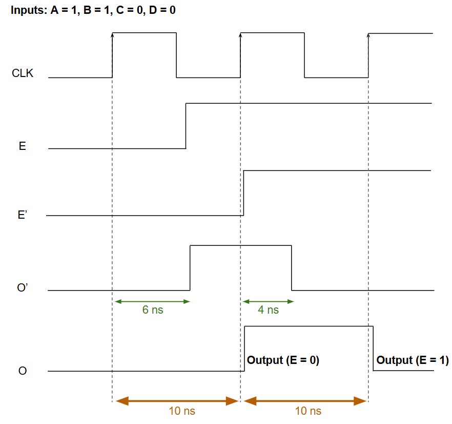
As you can see, E’ (output of register R0) and O (Output of register R1) do not change between clock cycles - this is important, because each of these signals can be used as part of other logic with the assumption that the data won’t change during the clock cycle - this is very important to make your designs larger without increasing the delays indefinitely. But this synchronization comes with strings attached, and my job is to ensure you abide by certain rules.
When I spoke about the role of registers in maintaining synchronization earlier, I might have given you the impression that registers are a gift from the heavens to save all digital designs. Maybe you think registers should be the ones doing the talking here. Let me tell you something, these registers aren’t as generous as you think. While registers help solve the synchronization problem, they introduce new problems in the process.
Remember how I said a register stores data when it sees the positive clock edge - I left out some of the nuances here. There are some registers out there that decide to store data at the negative clock edge instead, but everything that I talk about applies to those registers too - so let’s generalize by calling it a clock event. For the input data to be stored correctly at a clock event, the register enforces some strict rules. (Thanks again to the physics gods.) In my world, we use specific terms to express these “needs.”
The first term is Setup Time, which is the minimum time for which the input data to a register must be stable before a clock event. I’m not going to tell you the complete origin story of setup time here, but just know this - if you change the input to a register too close to a clock event, the registers cannot guarantee that they checked the correct value. Think of it like this - you are supposed to turn in your assignment by 10 AM, but you decide to make some last minute updates at 11 AM - a register is like that strict professor who says: “Sorry, I cannot promise that your updates would be graded.” Ah, if only registers were a good sport…
Their needs don’t end here - in addition to setup time, registers also have something called Hold Time - the minimum time for which the input data should be held stable after the clock event. This might seem excessive to you - this sounds like a professor who not only wants the assignment submitted by 10 AM, but also wants you to show up to their office, wait for 30 minutes while they review your assignment, and leave only after that. Seems unfair? I get it, but registers rule my world, and they are pretty high maintenance. You have no choice but to abide by their rules.
If you think our nightmare ends there, I’m sorry to burst your bubble. Remember that these registers, like everything else in a chip, work by moving electrons around. That means just like the cells we discussed earlier, they have propagation delays too. Typically, there are two different delays, since the path taken by the clock signal and input data are different. Here’s what we call them:
Clk→Q Delay: The delay in output resulting from the clock input
D → Q Delay: The delay in output resulting from the data input
Lot of information, huh? Looks like somebody needs help tracking all this. That’s where I come in. My job is to ensure that all the delays are accounted for, and the registers can guarantee that your design works as expected. The first thing I do, is call up my dear friend Dr. Morris Chang (or one of his friends that is going to manufacture this chip.) and get the setup time, hold time, and propagation delays of the registers. Remember, I already know the propagation delays of the other cells. With all this information, I’m like a fortune teller that can predict the future of your chip - except that unlike your fortune teller, I’m always right.
For me to check if your chip will work correctly, I need to ensure that your design meets all of the register’s needs. Let’s start by looking at setup time. Use the diagram below to follow along. To start with, I select a register, say R0 from the design, and pick one of it’s inputs - let’s call it In. At a positive clock edge, R0 stores the data from In. (When I do this analysis, I assume the input register, R0 in this case, does not violate Setup Time. This analysis is done for all registers, so trust me, it will all work out in the end.) Due to the propagation delay in R0, the stored data In’ is only seen after some delay. As I mentioned, a register can have two kinds of delays - but when I’m checking if setup time is met, I pick the larger of the two - because I want your chip to work under all circumstances. Once we get past R0, we see a familiar foe - the combinational delay which I spoke about in an earlier section. Adding both these delays gives us the time it takes to get the correct data for Out’ - the input to register R1. The register R1 expects to store this data at the next positive clock edge - it’s schedule is decided by the clock period. But as I mentioned earlier, the register does not like last minute changes to it’s input - so our real deadline is actually a little earlier than the next positive edge - to ensure that the data is held stable longer than the setup time of R1. This requirement can be expressed using fancy math operators, and this is called the Setup Time Constraint. My job is to check whether this constraint is met:
If YES, that means this path between In and Out “meets setup time”. The extra time you have before the setup time deadline is called Positive Slack.
If NO, the path “violates setup time.” The amount by which your delays exceed the deadline is called Negative Slack.
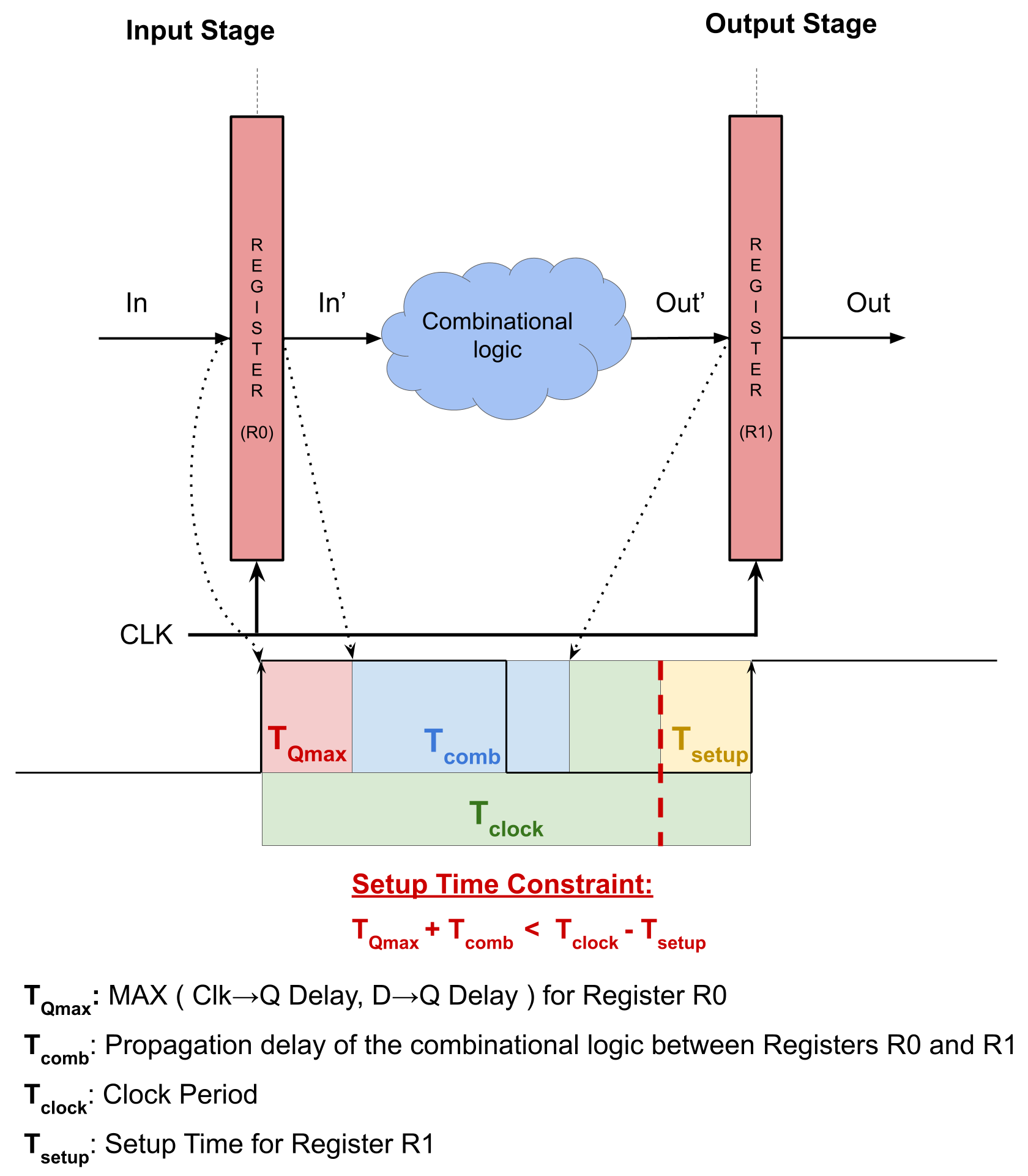
As I said earlier, registers also need data to be held for some time (called hold time) before it is safe for the input value to change. In the same scenario I described earlier for setup time, when the data from Out’ is being stored in register R1, a new value of In is being stored in R0, and then passing through the combinational logic to replace the current value at Out’. If this happens too fast, then the value of Out’ changes before the hold time of register R1 has passed - which would result in a Hold Time Violation. This gives me another constraint to check for - called the Hold Time Constraint. (You can think of it like a speeding ticket.) Similar to the setup time check, my goal is to ensure that the chip works at all circumstances - so when I am looking for a hold time violation, I take the smaller of the two propagation delays of register R0. Remember, smaller delays are bad when it comes to hold time.

Now that you know what I do, let me show you how I would actually do it, using the example design I described earlier. In this design, although there are just two registers, there are six different paths between inputs and outputs. (Four of them have unique combinational delays.) For each of these paths, I need to ensure that the setup and hold time constraints are met. Dr. Morris Chang was busy, so I made up some numbers for the register’s setup time , hold time , and propagation delays. With these numbers:
Path 2 and 3 meet both setup and hold time conditions - they are good to go
Path 1 fails setup time - it takes 8 ns for data to reach O’, but R1 expects it at 7 ns
Path 4 fails hold time - The path from E to O’ is just 4 ns long, giving R1 insufficient time to store the previous input
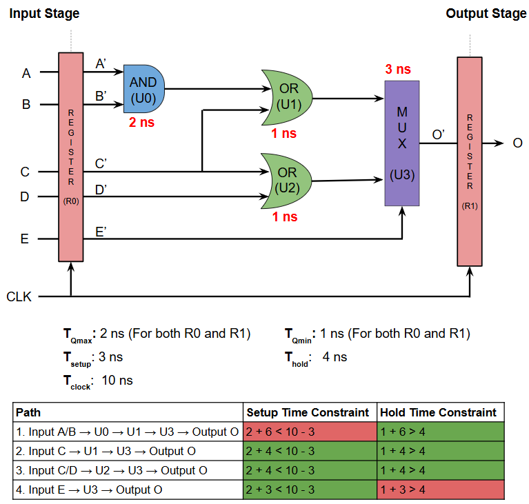
This analysis (i.e. Static Timing Analysis) clearly shows that this design does not pass timing. It also tells you exactly which paths are causing violations, and by how much. I have to repeat this analysis for every combination of input and output registers, and every possible path between the inputs and outputs. Even if one out of a million such paths has a setup or hold violation, I will find that for you, and prevent you from making a billion dollar mistake. That’s what makes me special…
Still not convinced of my value in your life? That’s okay, I have some more experiences to share from the real world that might just convince you. So share this story, and stay tuned for future installments of this series.