Translated from Zhihu article by “乱序摸鱼” (Out-of-Order Fish), Huawei Chip Architecture Evangelist
Original source: Zhihu Q&A on Huawei Kirin 2026 mobile chip with LogicFolding technology
[Note: Apologies for any errors due to translation.]
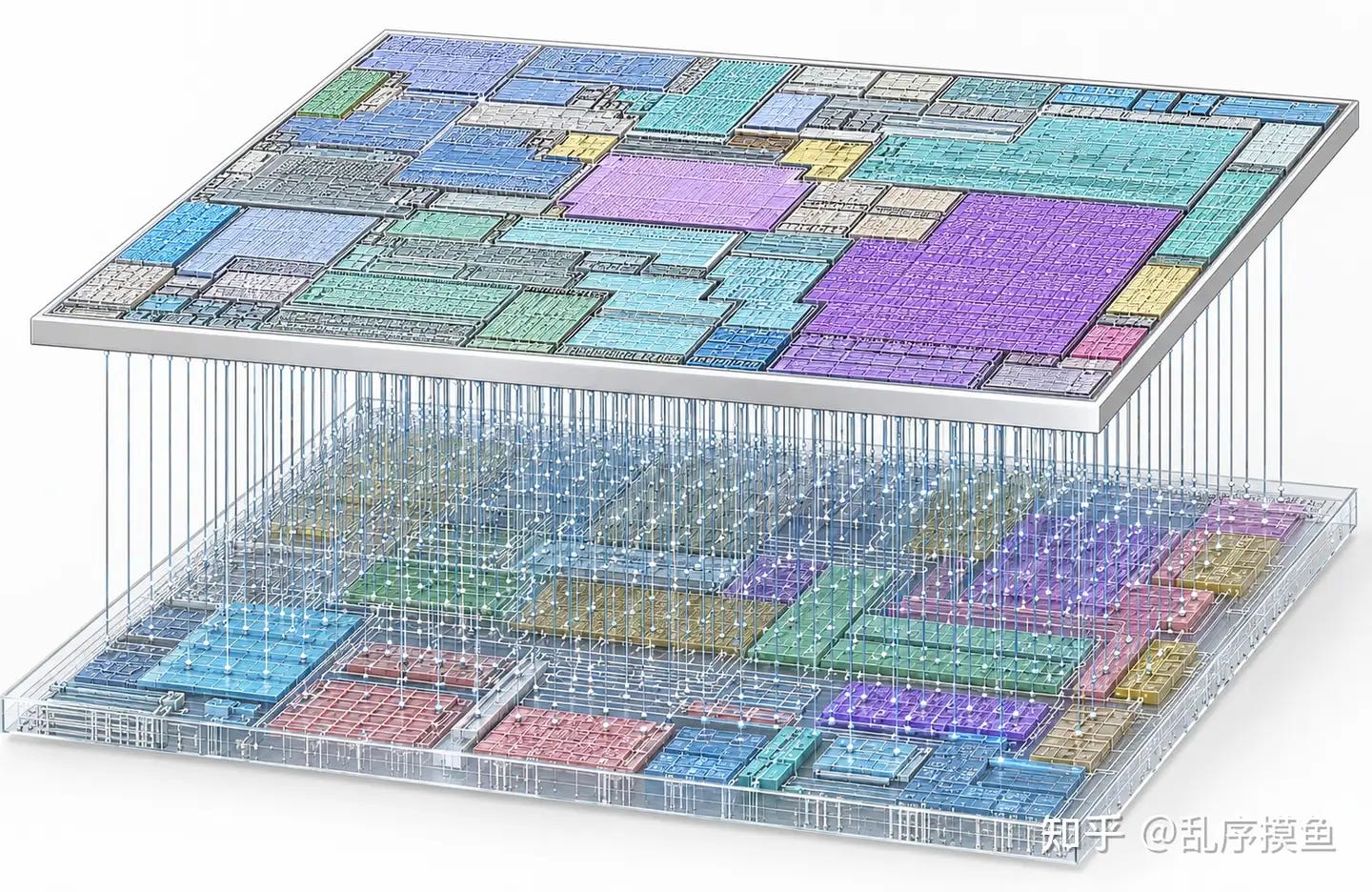
· Why Huawei can openly discuss LogicFolding
· Tau Law as systematic engineering (OS, ISA, IPs, EDA, DTCO, process, manufacturing)
· Space constraints in mobile phones
· Why traditional 2D scaling is unsustainable
· Wafer-to-wafer face-to-face (F2F) hybrid bonding
· Why not traditional 2.5D or chiplet approaches
· Yield and cost benefits
· Conservative choice matching top-level metal pitch
· TSV challenges (KOZ, stress, CMP)
· Need for DTCO and 3D-aware design flow
· 3D floorplan challenges
· Cross-die STA and timing closure
· Clock skew between dies
· Two approaches: antenna-style vs. local minimization
· Stagger hotspots, prioritize lower die heat paths
· From Temperature Sensor → Thermal Sensor
· Power Sensors and τ-DVFS
· HarmonyOS thermal digital twin
· 3D PDN design with TSV and hybrid bonding
· CPU: +44%, GPU: +87%, NPU: +213% by 2027
· Power efficiency similarly improved
· Logic folding proves 3D space as design space
· Not replacing Moore’s Law — complementing it
· Lessons for China’s semiconductor industry
Hello everyone, I’m the out-of-order fish, a chip architecture evangelist at Huawei. Today I’d like to talk about the design of Kirin 2026 and the story behind Tau Law (韬定律).
Why can we discuss these things openly? Because understanding the principles and actually building it are separated by an entire industrial chain. This isn’t false modesty — that’s just how chip engineering works. The menu can be public, the recipe can be explained, but to actually cook a full meal, you need ingredients, knife skills, heat control, stoves, and kitchen coordination. Every single one is indispensable.
Tau Law is not about any single point technology, but a systematic engineering effort: the HarmonyOS operating system, instruction set architecture, core IPs including CPU, NPU, and GPU, microarchitecture and RTL design, EDA tools, DTCO (Design-Technology Co-Optimization), process technology and manufacturing — none can be missing. If any link has a obvious weakness, the whole thing won’t work.
We architects may look like we’re slacking off, but what we’re actually doing is probing the system boundaries. We haven’t caught many fish, but we’ve certainly mapped out a lot of boundaries and... well, other things.
From Huawei’s internal mobile phone structure perspective, the Kirin SoC can be understood as the ‘central downtown’ of the phone. The CPU, GPU, NPU, ISP, baseband, security modules, caches, and interconnect networks all need to be crammed into this single piece of silicon. But it’s not a standalone villa. It has to share space on the phone’s mainboard with the battery, camera modules, high-speed UFS storage, power management chips, RF front-ends, and numerous discrete components — all competing for space on this inch-of-gold real estate
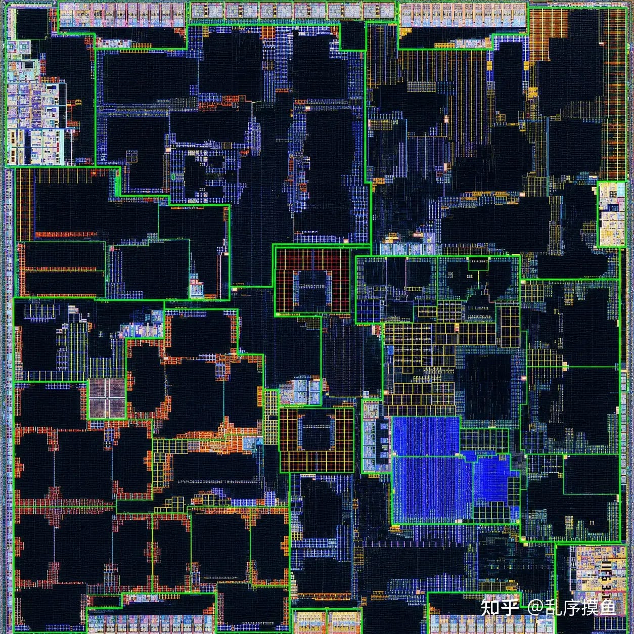
.
Mobile phones are getting thinner and lighter, cameras are multiplying, batteries are getting larger, and RF systems are becoming more complex. The space left for SoC packaging is extremely tight. The mainboard is like a small room already stuffed with furniture — you want a bigger sofa, a bigger refrigerator, and a bigger bed, only to find there’s no room left to turn around.
If you want to increase the SoC area, you have to increase the phone’s length, width, or thickness, or squeeze the battery space. But phones are already quite large, and significant increases are basically impossible. Battery energy density is also hard to keep improving rapidly. Performance improvements bring higher power consumption, yet users want longer battery life, so battery space cannot be easily reduced.
This is awkward. Users want Huawei phones to be faster, cooler, thinner, lighter, with longer battery life, better cameras, smarter AI — and preferably without a price increase. After hearing this, Huawei engineers usually go silent for three seconds, then look at their year-end bonuses, worrying about whether they can last a few more years and whether they’ll get their contracts renewed.
Therefore, the traditional path of increasing chip area to accommodate more transistors is becoming increasingly difficult to sustain in mobile devices. In an era where Moore’s Law is slowing down, moving from planar to stacked is an important direction.
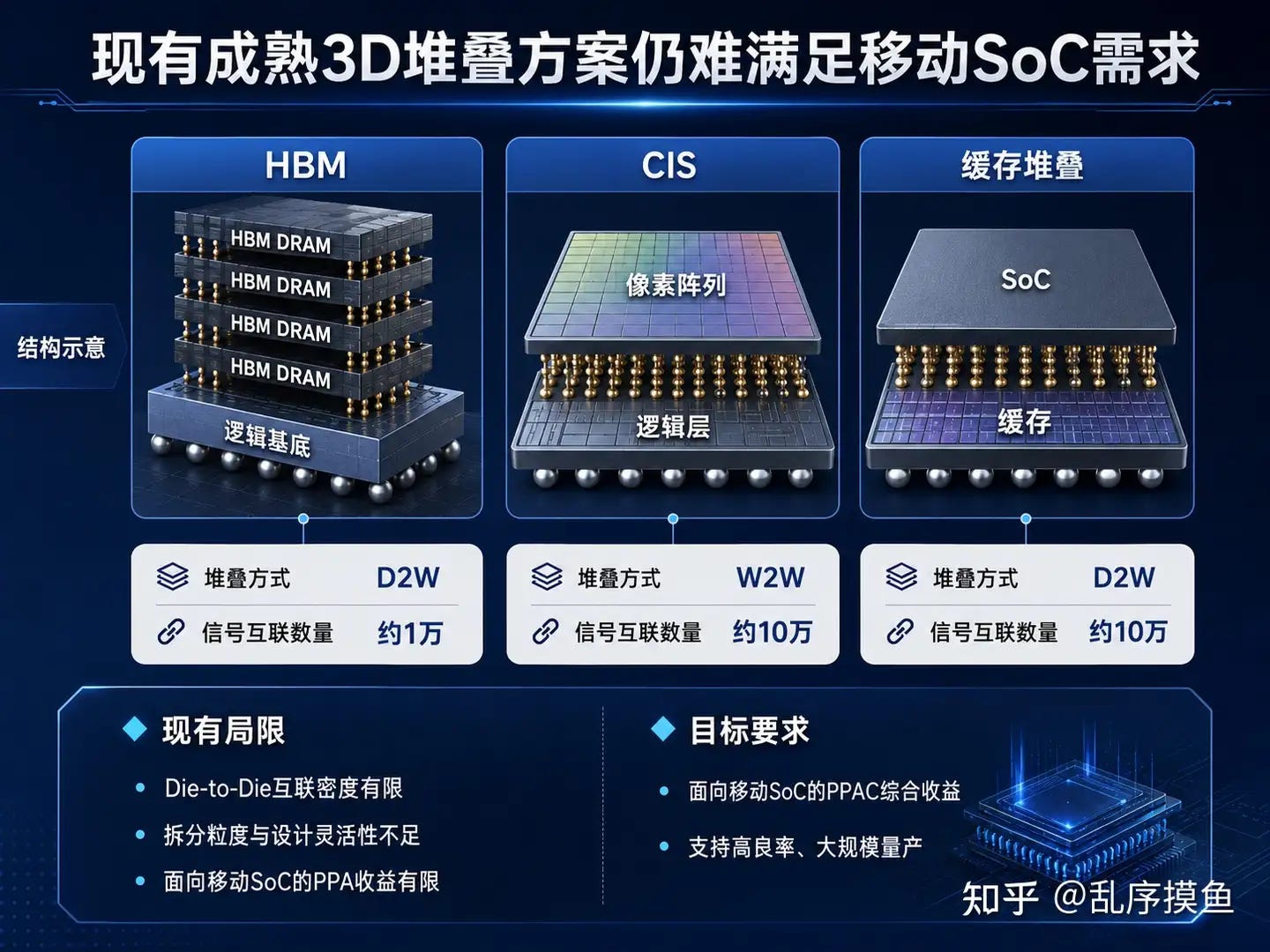
Of course, Huawei wasn’t the first to see 3D stacking. Apple, Qualcomm, AMD, Intel, and TSMC have been exploring advanced packaging, chiplet interconnection, 3D stacking, and hybrid bonding earlier and more maturely than us.
Apple’s UltraFusion has already turned two large dies into a unified SoC through high-density interconnection. AMD’s 3D V-Cache has long stacked cache vertically above the CPU and has entered multiple product generations. Intel’s Foveros and Foveros Direct have moved from 2.5D, 3D packaging all the way to copper-copper hybrid bonding. TSMC, needless to say, has consolidated SoIC, CoWoS, and InFO capabilities into its 3DFabric platform, providing customers with complete 3D system integration solutions. Qualcomm, though less public about its products than AMD and Intel, has also had early patent and technology layouts in monolithic 3D IC for mobile SoCs, vertical memory, and multi-layer logic integration.
So don’t think the industry doesn’t understand 3D IC, and don’t think only Huawei thought of stacking. Even more, don’t simplistically say others are just piling chips on top of each other. On the contrary, many industry solutions entered engineering validation and product verification earlier than Kirin, with more stable roadmaps and thicker experience
.
But the stacking technology we’re showing this time is indeed quite different from traditional players’ paths. Many other solutions stack around relatively well-defined modules like cache, memory, sensors, and chiplet interconnection. What Kirin 2026 wants to prove is: in a mobile SoC space that’s so small, so hot, and so competitive, can we do fine-grained folding of large-scale logic circuits, so that CPU, GPU, NPU, cache, and interconnect are no longer just spread out on a plane, but reorganized in three-dimensional space?
The difficulty is that this is not a pure packaging problem, nor is it as simple as sticking two dies together. It requires architecture, circuit design, physical design, EDA, process, packaging, testing, and mass production to all be calculated together. If any link falls behind, what starts as an ‘advanced architecture’ in PowerPoint ends up as an ‘advanced sample’ in the lab.
Huawei HiSilicon over the years, under external pressure, has gradually been pushed into an organizational form approximating an IDM (Integrated Device Manufacturer). An IDM means deeply participating in chip design while also mastering or coordinating process manufacturing, packaging testing, and production ramp-up. We’re not like a pure design house that only needs to draw pretty schematics; nor are we like a pure foundry mainly responsible for process stability. What we need to do is pull design, process, manufacturing, packaging, testing, and production ramp-up all to one table, argue it out, and then still make the thing together.
This game is not fun — high barriers, many pitfalls. Others are like students who went through elementary school, middle school, and high school with solid foundations and rich competition experience. We’re more like being grabbed halfway to participate in the Olympiad, skipping the college entrance exam, but still getting the direct admission qualification, jumping several grades to enter university.
So, whether it’s Apple, Qualcomm, or TSMC behind them, their accumulated experience in 3D chips is deeper than Huawei HiSilicon’s. There’s nothing wrong with admitting this. We haven’t been in this game that long, and many capabilities were forced to grow by reality. Precisely because of this, we can’t rely on a single point breakthrough, but must take the system engineering route: linking operating system, instruction set, architecture, chip design, EDA, process, packaging, testing, and production ramp-up together.
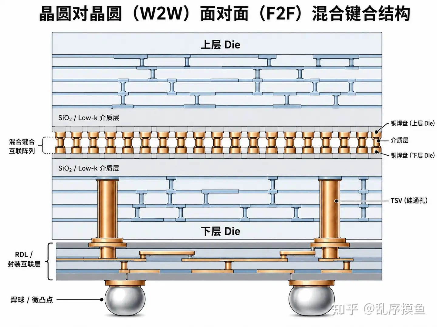
Simply put, Kirin 2026 stacks two wafers face-to-face. Face-to-face means face-to-face, which is F2F (Face-to-Face). In between, hybrid bonding is used to connect the upper and lower layers with ultra-high-density interconnection. The backside of the bottom wafer then uses TSV (Through-Silicon Vias) to continue routing signals, power, and ground outward.
If you just go the traditional 2.5D route, putting several chiplets on the same interposer or package substrate, the advantage is maturity and flexibility — bad dies can be screened out, yield pressure is relatively small. HBM, GPUs, and AI accelerators mostly follow this approach. But its problem is also obvious: it’s more suitable for module-level interconnection, not for fine-grained logic folding. Because the distance between dies is still relatively long, and interconnection density isn’t high enough. It’s like putting several buildings in the same complex with highways between them — throughput can be large, but you can’t expect every office to be as close as upstairs and downstairs.
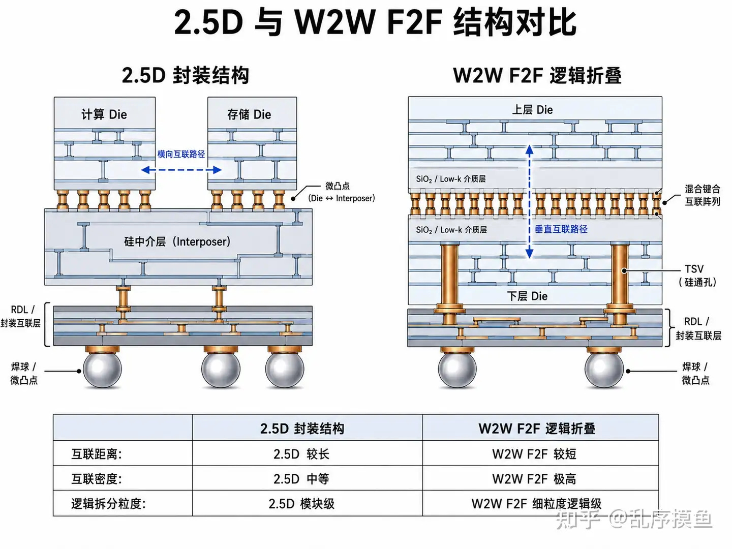
If using die-to-die chiplet approach, sticking known-good dies together is more stable in engineering and offers more combination freedom. But the cost is that interconnection pitch is usually not fine enough, and package area tends to grow larger. For servers and high-performance computing, this trade-off might be worthwhile. But for mobile SoCs, space is too tight, power is too sensitive, and latency is too demanding. Mobile SoCs don’t need occasional communication between a few large modules — they need CPU, GPU, NPU, cache, and interconnect network interacting at high frequency every day. Once interconnection is too coarse, logic can’t be split finely; logic can’t be split finely, there’s no talk of real folding.
Wafer-to-wafer’s advantage is that two whole wafers are aligned and bonded in one go. Unlike sticking die by die slowly, it’s two large ‘chip motherboards’ directly merging. This is efficient, has high interconnection density, and is more suitable for high-volume mobile SoCs. Of course, the downside is also real: once certain areas have defects, the impact could be on a whole wafer. So it has very high requirements for yield, alignment, flatness, and process control. In short, this isn’t the easiest path, but it’s the one most likely to fold logic finely.
But further analysis shows that yield might not actually get worse — on the contrary, there are opportunities for yield and cost benefits, mainly for three reasons. First, after logic folding, the dimensions of upper and lower dies are significantly reduced, single-die yield improves, so overall yield can be comparable to 2D (two-dimensional planar chip) solutions. Second, the additional yield loss introduced by high-yield, high-efficiency folding processes is already almost negligible. Third, combining 2D-friendly design approaches and fully utilizing each layer’s process advantages can yield yield and cost benefits relative to 2D solutions. Actual product results also show that compared to 2D solutions, logic folding can achieve good cost benefits.
The value of F2F (Face-to-Face) is that the front sides of two logic layers face each other directly. The front side of a chip has transistors and multi-layer metal interconnect. After front-to-front alignment, the distance between upper and lower layers can be very short. It’s like two office buildings not being connected by a skybridge across a road, but directly aligning the floors with doors in between. Originally a department had to run to the neighboring complex for meetings; now it’s just going upstairs or downstairs — shorter path, less time.
Ultra-high vertical interconnection density enables a good matching relationship between hybrid bonding pitch and top-level metal pitch — what’s called the ‘meshing ratio.’ In plain terms, the density of upper and lower interconnection points needs to match the chip’s internal wiring scale. If interconnection points are too sparse, it’s like a city with only a few bridges across the river — all cars have to detour and queue. If interconnection points are dense enough, it’s like having tunnels, elevators, and subway entrances everywhere — the city’s transportation truly becomes three-dimensional. After folding, the upper die and lower die no longer form independent modules, independent subsystems, or independent SoCs. Instead, upper and lower dies form modules, subsystems, and a complete SoC together through massive interconnection.
Pitch, in plain terms, is the spacing between copper pads on the upper and lower layers. The smaller the pitch, the more vertical interconnection points per unit area, and the more boldly logic can be split finely. But the cost is direct: alignment needs to be more precise, surfaces need to be flatter, defects need to be fewer, and yield pressure is greater.
Kirin achieving 1.5μm pitch this time is already very strong, but I actually think it’s a conservative choice.
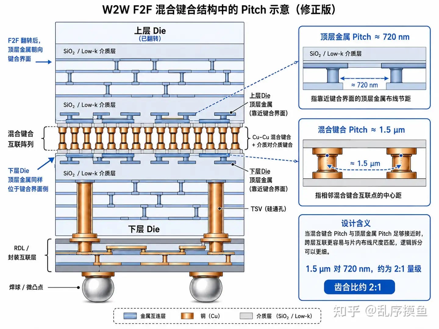
Why do I say this? Because what logic folding truly values is not just how small the pitch itself is, but whether it matches the top-level metal wiring scale. Top-level metal pitch is around the 720nm magnitude. If hybrid bonding pitch is too large, even though upper and lower layers are stuck together, the connection points are too sparse, and many signals still have to take detours. That’s like a city with only a few bridges across the river — theoretically the two banks are connected, but in reality everyone is stuck in bridge traffic every day.
1.5μm is roughly twice the top-level metal pitch. This density is already sufficient for fine-grained splitting of key logic, but it hasn’t pursued the extreme one-to-one matching. In other words, it’s not the most aggressive solution, but a relatively stable point between ‘interconnection density’ and ‘process manufacturability.’
This point is very important. Because logic folding is not like memory arrays. If a few cells in a memory array go bad, they can be replaced with redundant cells. Logic circuits are much more troublesome — many connections are unique. If a critical path is broken, it’s not a matter of losing a few parking spaces; it’s like a section of the city’s overpass collapsing, potentially paralyzing the entire traffic system.
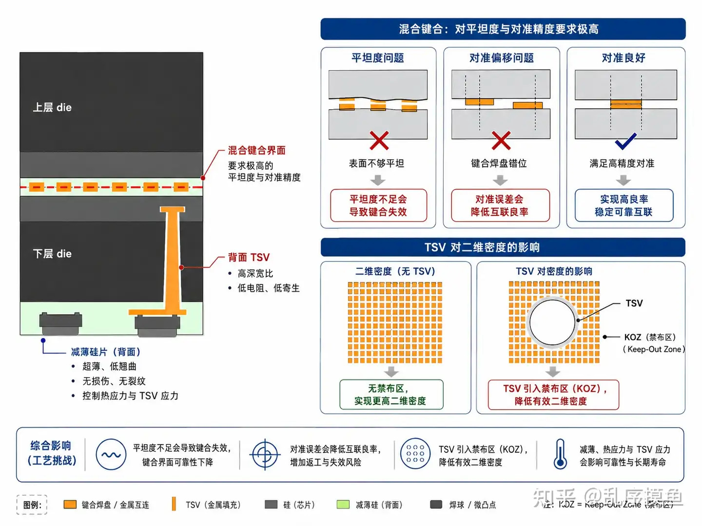
So this can’t be left to chance. Once wafer-to-wafer is bonded, two whole wafers are stuck together. Hybrid bonding requires copper-to-copper and dielectric-to-dielectric bonding simultaneously. Slightly uneven surfaces or slightly off alignment can cause bonding voids, connection failures, or reliability issues. When we misalign our phone screen protectors, we can peel them off and reapply. Wafer bonding is not so gentle — it’s basically a lifetime commitment.
TSV is the same. It looks like drilling a vertical shaft in a silicon wafer, but engineering-wise it’s far from that simple. The holes need to be deep and straight, going through different material layers, then insulated, blocked, and filled, without voids, cracks, or stress issues. It’s a bit like drilling vertically through a thousand-layer cake — each layer has a different temperament, and you can’t crush, cut crooked, or break the cake.
So Kirin didn’t max out all risks in this generation. Pitch at 1.5μm, TSV dimensions and landing relatively conservative, logic folding prioritized on critical paths rather than reconstructing the entire SoC all at once. In plain terms: fold the places most worth folding first, get the performance, power, and area benefits first, while keeping yield and mass production risks under control.
Architects, of course, all want to do it in one step — best to finish the drawing today, double performance tomorrow, and halve power the day after. But process engineers will generally calmly remind you: survive first, secure this year’s year-end bonus, then talk about ideals.
Also, 3D stacking isn’t just about adding one more layer in the vertical direction. It affects the manufacturability and device performance of the original 2D chip.
The most typical example is TSV. It looks like drilling a few ‘elevator shafts’ into the chip, but these elevator shafts don’t come from nowhere. They take up space, change surrounding pattern density, and also affect CMP (Chemical Mechanical Planarization). CMP can be understood as the process of ‘grinding flat’ the wafer surface. Where there’s more metal, where there’s more dielectric, all affect the final flatness. Once TSVs are added, the relatively uniform pattern density in the original 2D design is disrupted, and subsequent flatness, thickness control, and bonding quality are all affected.
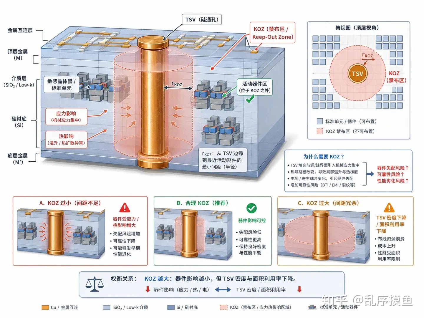
TSV also has an unavoidable problem: stress. TSVs are typically copper, surrounded by silicon. Copper and silicon expand differently when heated. Thermal expansion and contraction back and forth create local stress around the TSV. This stress affects the performance and reliability of nearby transistors. Mild cases cause parameter drift; severe cases cause yield and lifetime issues.
So the design must reserve KOZ (Keep-Out Zone) for TSVs. Simply put, a safety distance must be left around TSVs — don’t put sensitive transistors too close. The larger the KOZ, the less TSV affects devices. But if KOZ is too large, TSV density can’t go up, and area utilization drops. It’s like building subway shafts in a city — too little safety distance, neighboring buildings are affected; too much safety distance, and downtown land is wasted.
This is the most troublesome part of 3D IC: many problems can’t be solved by optimizing in isolation. TSV size, KOZ size, bonding pitch, pattern density, CMP, thermal budget, stress, yield, and area utilization are all tied together. You move one, and the others follow. So DTCO (Design-Technology Co-Optimization) is essential. Design can’t just care about ‘how I want to connect’; process can’t just care about ‘what I can do.’ Both sides have to calculate the bill together.
Heat treatment and wafer thinning are similar. During 3D stacking, there are bonding, annealing, thinning, and re-interconnection steps, all of which bring additional stress to transistors and metal interconnect. Too high temperatures may affect device characteristics and low-k dielectric reliability; wafers ground too thin are prone to warping, cracking, and stress. So logic folding typically requires low-temperature stacking processes. Low temperature sounds gentler, but process difficulty doesn’t decrease — on the contrary, it requires cleaner surfaces, more precise alignment, and more stable bonding interfaces.
Therefore, logic folding is not a simple splicing of two dies, but requires a design flow with true 3D awareness. This flow must know the physical positions of upper and lower layers, interconnection costs, thermal distribution, power supply impact, and process constraints from the very beginning. Only then can logic folding avoid being a 2D problem moved into 3D space to continue suffering, and truly turn 3D space into a new degree of freedom for performance, power, and area optimization.
The rough construction is done — what’s next? Interior decoration.
Logic folding is the same. Earlier we stuck two dies together through hybrid bonding, TSVs are connected, and it looks like the building is done. But a building being done doesn’t mean it’s livable. The real difficulty is: which room is the bedroom, which is the kitchen, which is the bathroom, where does water and electricity come from, where are the stairs, where to hang the air conditioner outdoor unit, how to dissipate heat, and how to repair things when they break later.
Floorplan is dividing the large rooms, deciding how to place large blocks like CPU, GPU, NPU, and SRAM. Placement is putting furniture in the rooms, placing standard cells and macro modules. Routing is wiring, connecting all the electrical wires, water pipes, and network cables. CTS is clock tree synthesis, responsible for delivering the clock signal to each flip-flop so everyone hears the ‘work bell’ at roughly the same time.
The real partition is the most critical step in 3D chip design. It basically determines the ceiling of this chip.
Because whether the upper and lower layer areas can be fully utilized depends on it. Whether originally long critical paths can be shortened depends on it. Whether hotspots will stack on top of each other depends on it. How power is delivered, how clocks are routed, whether hybrid bonding points are sufficient, where TSVs are placed, and whether subsequent routing will be congested — all relate to it.
So partition is not a simple ‘module splitting’ problem. It’s more like decorating a duplex apartment. Where you put the bedroom isn’t just about sleeping — it also affects lighting, wiring, drainage, load-bearing, noise, and later maintenance. Chips are the same. Putting a certain module on the upper layer might shorten critical paths, but it might also increase cross-die interconnection, make power delivery harder, concentrate heat more, and clog routing completely.
In traditional 2D SoCs, this process, though also iterative, is still relatively linear. First define architecture, then write RTL, then synthesize, then floorplan, placement, CTS, routing, and finally signoff for the full physical check. RTL can be understood as the construction drawing of chip logic; signoff is the full physical examination before handover.
But after logic folding, this process is no longer a straight line — it becomes a strongly coupled closed loop. You do partition first, then floorplan might say it can’t fit; placement might say it’s too congested; PDN might say voltage is dropping here; thermal analysis might say these two hotspots are directly above and below each other, like two hotpot restaurants on upper and lower floors both running at maximum fire; STA might say cross-die timing can’t be closed. Finally, everyone looks around and goes back to change the partition.
This is the most torturous part. Rework in the 2D era was already painful enough; in the 3D era it’s 3D rework. You move one module, and heat, power supply, timing, routing, and yield might all move together. The architect originally just wanted to shorten a long path, but EDA, physical design, process, packaging, and testing all stand up and say: hold on a minute.
And honestly, there weren’t mature tool chains waiting for us from the start. Traditional EDA tools grew primarily for 2D design. Their worldview is a flat city map. Now we suddenly ask them to understand duplex apartments, underground garages, elevator shafts, plumbing, and fire exits — they certainly can’t be smooth immediately. Many judgments can only rely on architecture experience, physical design experience, and process experience, trying round after round, pushing version after version, hitting walls again and again. This process is not romantic. It’s not drawing a 3D arrow in PowerPoint and then performance goes up.
The reality is: today timing can’t close, tomorrow routing is congested, the day after thermal analysis explodes, and the day after that power supply paths aren’t thick enough. Many solutions look beautiful but reveal their true form after signoff. We weren’t born knowing this either — it was after being ground into the dirt by problems that we slowly figured it out, bit by bit. One of the hardest examination items is cross-die STA.
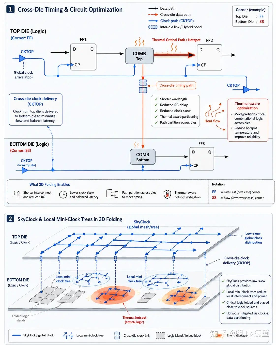
What about clocks on upper and lower dies?
This question is actually particularly critical. Because a chip isn’t a bunch of logic gates calculating on their own — it’s more like a company where all departments listen to the same work bell. When the bell rings, data starts moving; when the next bell rings, data must arrive on time. Too early is no good, too late is no good either.
In 2D chips, this is already difficult. In logic folding, it’s even more troublesome. Because now the company doesn’t operate on one floor — upper die and lower die are separate offices, connected by hybrid bonding and TSV. People can go up and down stairs, but when the bell reaches each floor must be redesigned.
Here we need to talk about clock skew.
Clock skew is the time difference when the same clock signal arrives at different flip-flops. Flip-flops can be understood as ‘small gates’ in the chip. When the clock comes, it decides whether data is released or locked. Ideally all gates hear the bell simultaneously; in reality, some places are earlier, some later. If the difference is too large, data might be late or early. Being late is a setup violation; being early is a hold violation. Neither is funny — both can cause chip malfunctions.
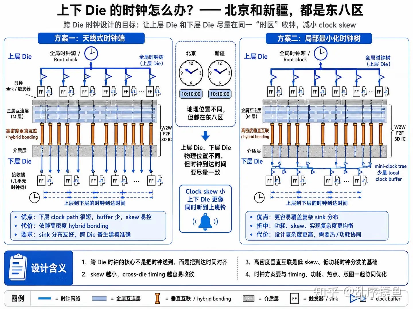
So the core of cross-die clock design is not simply ‘sending the clock to the lower die,’ but making the upper die and lower die work as much as possible on the same beat.
This is like Beijing and Xinjiang. Geographically far apart, the perceived sunrise time is different, but administratively both are UTC+8. For chips, the physical positions of upper die and lower die are different, paths are different, and temperature, voltage, and process conditions may differ, but from a timing perspective, they should ideally all receive the clock as if in the same time zone.
This sounds easy but is extremely torturous in practice.
Because in cross-die paths, both clock paths and data paths become more complex. Data might be computed halfway on the upper die, then go through hybrid bonding to the lower die. The clock might also be distributed from the upper die and then vertically delivered to the lower die. There are metal wire delays, buffer delays, hybrid bonding parasitic parameters, and upper and lower die voltage droop, temperature differences, and PVT mismatch. If you miscalculate slightly, setup margin and hold margin get eaten up.
To reduce clock skew, we have roughly two classes of approaches.
The first can be called the antenna-style clock termination scheme.
This approach’s idea is straightforward: the global clock tree is mainly placed on the upper die. The lower die tries not to grow a complete clock tree, but instead uses high-density hybrid bonding to deliver the clock directly near the lower die flip-flops, like an ‘antenna probing down.’ The lower die is more like a receiver, with fewer buffers, less routing, and shorter clock paths.
Its benefit is obvious: lower die clock paths are short, buffers are few, clock latency differences are small, and skew is easier to control. Like the whole building using one unified broadcast system, then each floor only has very short speaker lines, so everyone hears the bell more consistently.
But its cost is also obvious. It heavily depends on high-density vertical interconnection. If hybrid bonding points aren’t dense enough, the clock can’t be delivered wherever you want. If sink distribution is unfavorable — meaning flip-flops are too scattered — vertical drop points are hard to arrange. If cross-die parasitic parameter modeling is inaccurate, everyone might hear the bell simultaneously in simulation, but on the real chip some might hear it early and some late.
So this scheme isn’t simple and easy — it pushes the difficulty onto hybrid bonding density, sink planning, and parasitic modeling.
The second approach is the local minimization clock tree scheme.
It’s not so extreme. The global clock is still mainly distributed on the upper die, then delivered to the lower die through vertical interconnection. But the lower die no longer completely receives bare — it retains a small number of local clock buffers, making a very small mini-clock tree. The upper layer is responsible for unified command; the lower layer is responsible for local fine-tuning.
This scheme is more like building broadcast in reality. The main control room is upstairs, but certain areas downstairs are too complex with too many rooms, so a few small splitters are added downstairs to make bell coverage more even.
Its benefit is that it’s easier to cover complex sink distributions, without requiring all flip-flops to grow right next to vertical interconnection points. It’s also easier to trade off between power consumption, skew, and implementation complexity. But the cost is more buffers on the lower die, more local clock trees, higher power consumption, possible local hotspots, and higher design complexity.
So neither scheme is absolutely better or worse. The antenna scheme is cleaner, easier to control skew, but requires ideal vertical interconnection density and layout distribution. The local minimization clock tree is more engineering-oriented, more adaptable, but at the cost of power consumption, area, and complexity.
The truly difficult part is that we can’t look at the clock alone. The clock scheme must be considered together with timing, power consumption, heat, floorplan, and placement. If you add more buffers somewhere to reduce skew, timing might improve but power goes up; power goes up, hotspots come; hotspots come, transistors slow down, and timing breaks again. The most annoying part of chip design is right here: you hold down one gourd, and a row of floating gourds pop up beside it.

When people hear about logic folding, the easiest question to ask is: after folding, what about heat dissipation?
This question is very accurate. Because what 3D chips fear most is not ‘can’t stack’ — it’s becoming a small furnace after stacking. Transistor density goes up, power density may follow. Mobile SoCs aren’t servers — you can’t hang a big fan next to them. You run benchmarks fiercely for the first ten seconds, then throttle after heating up, games start dropping frames, AI inference starts jittering, and the phone feels like a hand warmer in your palm. Users won’t care how many die layers you used — they’ll just think this thing is hot.
So, heat dissipation is not an extra credit question for logic folding — it’s a main question. You could even say this is one of the true core competitive advantages of Tau Law.
Tau Law doesn’t simply say ‘I want to stack more transistors.’ If you just compress more transistors into a smaller area, it’s easy to turn a furnace into a double-decker furnace. What Tau Law truly wants to do is: through logic folding, shorten signal paths, reduce long connections, lower RC, reduce buffers and repeaters, so the same computation walks less, moves less data, and consumes less power.
Where does heat come from? Ultimately it’s energy consumption. Every time a signal runs a segment of wire, capacitors charge and discharge. The longer the wire, the larger the RC, the higher the power consumption. Logic folding turns originally long-distance commutes on a 2D plane into short-distance direct routes upstairs and downstairs. Shorter path, less traffic jams, less fuel burned. Corresponding to the chip, this means interconnect energy consumption decreases, local communication becomes more efficient, and heat generated per unit performance also has a chance to come down.
Of course, between hybrid bonding pitches, there are thermal conduction trenches — this is equivalent to adding ventilation and water systems between the two chips, allowing heat to be expelled as much as possible.
However, heat dissipation can’t rely solely on these heat sinks and conduction trenches for remediation. That’s like finishing house decoration only to discover the kitchen has no exhaust duct and the bathroom has no drainage, then saying ‘let’s buy an air purifier.’ Useless — the root is wrong.
The true core of logic folding’s thermal design must enter the partition, floorplan, and placement design methodology from the very beginning of chip design.
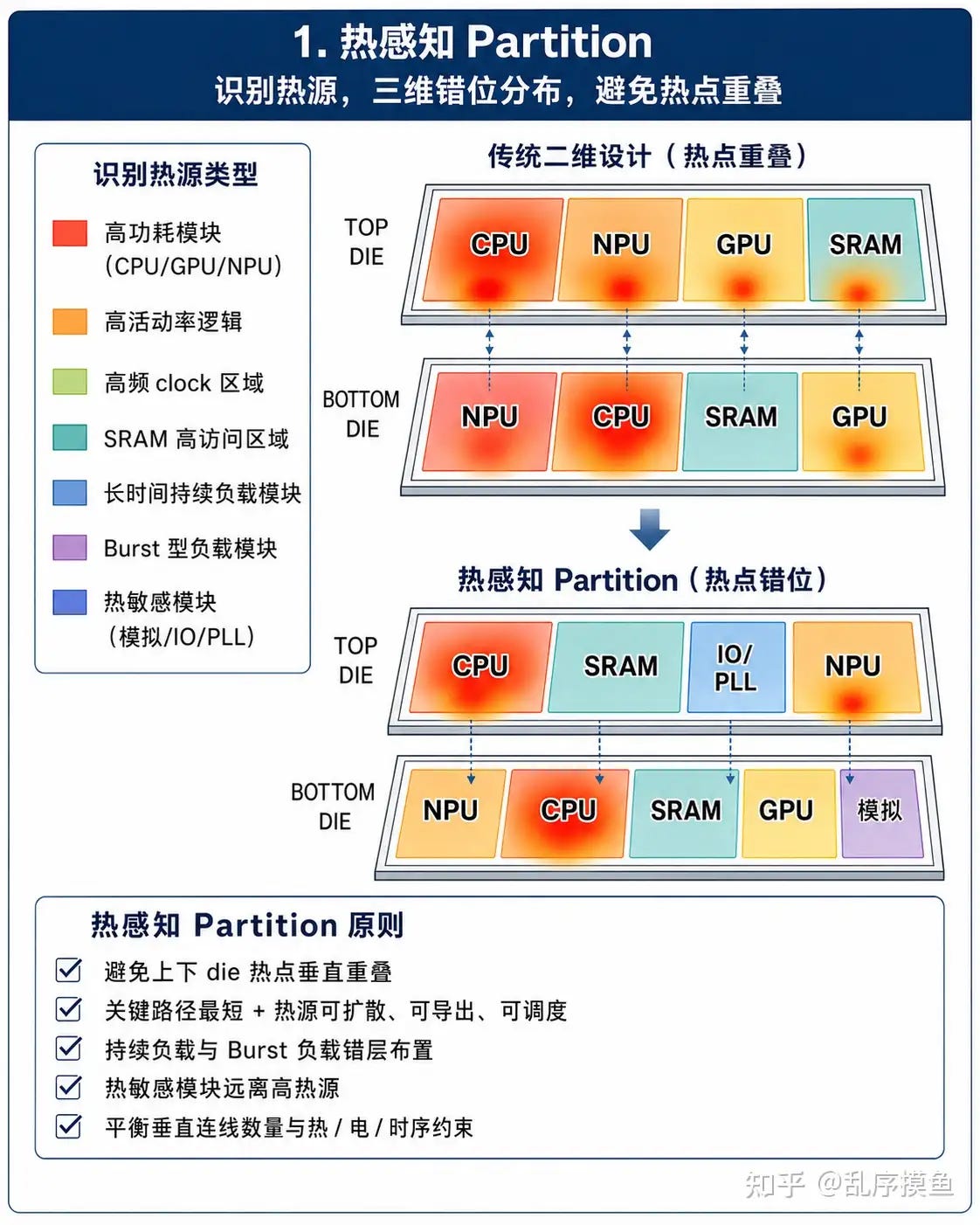
At the partition stage, you must first judge: which modules are furnaces, and which are just small desk lamps. CPU, GPU, NPU, high-frequency clock regions, and high-access SRAM are all potential heat sources. In traditional 2D design, if these modules aren’t placed well, at worst there’s local overheating on the plane. In 3D, if upper and lower die hotspots happen to overlap, it’s not one furnace — it’s two hotpot restaurants on upper and lower floors running at maximum fire simultaneously.
So the first principle is: hotspots must be staggered. Don’t put CPU directly above NPU. Don’t vertically overlap high-activity GPU regions with high-access SRAM. Don’t stack high-frequency clock regions above another high-power module. Like decorating a duplex apartment, you can’t stack kitchens on both upper and lower floors in the same corner — grease, heat, water, and electricity all crowded there will definitely be uncomfortable later.
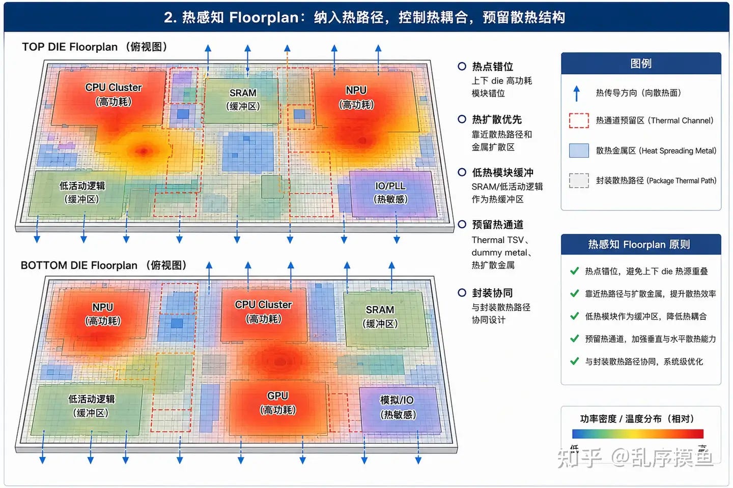
The second problem is that the lower die’s heat dissipation path is worse. The upper die is closer to the system heat dissipation path. The lower die’s heat must pass through the bonding interface, dielectric layer, upper die, and packaging material before it can escape. It’s like opening a hotpot restaurant in the basement — heat isn’t impossible to exhaust, but it’s definitely harder than on the first floor. So when we do floorplan, we can’t just look at whether paths are short — we also need to see whether heat has a path to go. High-power modules should be placed as close as possible to better heat dissipation paths. Low-power modules can serve as buffer zones in the middle. When necessary, auxiliary structures like heat channels, dummy metal, and thermal TSVs must be reserved.
The third problem is that after dies become thinner, lateral heat spreading capability weakens. Thinner silicon wafers are good for stacking and vertical interconnection, but heat diffusion capability in the plane decreases, and hotspots become sharper. You can understand it like teppanyaki using a thick iron plate — heat spreads out. If the iron plate becomes a thin sheet, local spots are more likely to burn a point. So at the placement stage, you can’t just shorten wirelength by stuffing high-activity logic, clock buffers, and critical path cells all together. Paths are shorter, but heat and IR drop might explode together.
At the partition stage, first identify heat sources: high-power CPU clusters, high-activity GPUs, continuously running NPUs, high-frequency clock regions, high-access SRAM, and burst-type power modules. Then distribute them in 3D space with offset positions, avoiding vertical overlap of upper and lower die hotspots.
The principle is simple: don’t stack two furnaces on top of each other. CPU clusters shouldn’t be directly above NPU high-activity areas. High-frequency clock regions shouldn’t be stacked above high-access SRAM. Continuous loads and burst loads can be arranged on different layers. PLL, analog, and IO — these heat-sensitive modules should avoid large heat sources as much as possible.
At the floorplan stage, continue considering heat paths. High-power modules should be close to heat dissipation paths, metal-dense areas, or heat spreading structures. Low-power logic and low-activity SRAM can serve as buffer zones. When necessary, reserve space for thermal vias, thermal TSVs, dummy metal, and heat spreading metal. You can’t wait until the chip is almost done before remembering ‘isn’t this a bit hot?’ At that point it’s like finishing house decoration before discovering the kitchen has no exhaust duct — you can basically only pray for neighborly tolerance.
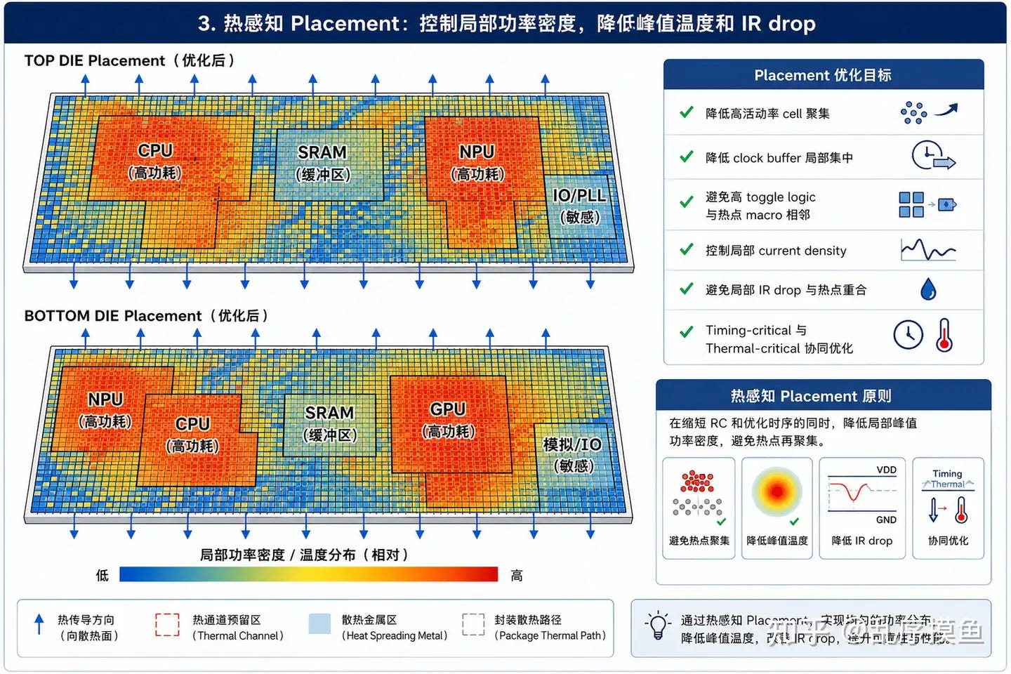
At the placement stage, control cell-level local power density. Don’t stuff high-toggle logic, clock buffers, and timing-critical cells all in one corner just to shorten wirelength. Paths are shorter, but local heat and IR drop might explode together. Truly good placement shortens RC while keeping local peak power density down.
System-level heat dissipation must also be considered together. How does the top die’s path to the heat spreader go? Can low thermal resistance channels be placed above bottom die heat sources? How to reduce TIM interface thermal resistance? How to use thermal TSVs or dummy TSVs? How to choose die thinning thickness? How do VC, graphite, and metal frames in the phone cooperate? How does system scheduling avoid CPU, GPU, and NPU peaking simultaneously? All of these must be calculated together.
The ultimate goal is not to make instantaneous temperature look a bit better, but to reduce peak power density under thermal steady state, delay thermal throttling trigger time, and improve sustained performance. What users truly perceive is not what peak score you ran at the product launch, but whether it’s still stable after playing for half an hour.
After logic folding, power supply is more complex than 2D SoC. The reason is simple: the building became three-dimensional, and electricity also needs three-dimensional supply.
In traditional 2D design, top-level metal mainly serves power, ground, long-distance signals, clock trunks, and large-bandwidth buses. After logic folding, top-level metal also has to carry large amounts of cross-die signals, hybrid bonding landings, TSV landings, and global routing channels. Everyone wants top-level metal because there the line width, impedance, and routing resources are better. In the end it’s like downtown main roads — buses need to go, trucks need to go, ambulances need to go, and leadership convoys need to go. Of course it’s congested.
Tens of millions of hybrid bonding interconnections can’t be planned by hand. Which points go to signals, which to power, which to ground, which to clocks, which areas are reserved for TSVs, which areas avoid hotspots and KOZs — all need automated coordination.
What’s more troublesome is that the lower die often doesn’t just power itself — it also has to supply power to the upper die through vertical channels. This way the bottom die’s PDN current density increases, and upper and lower die power demands may also be spatially inconsistent. A high-power area on the upper die might project to a weak power supply area on the lower die. When upper die load jumps, lower die power also jitters. Power supply noise might even propagate across dies.
So upper and lower die PDNs can’t be designed separately. A complete 3D power integrity flow must be established.
The complete power supply path is roughly: package bump comes in, through RDL and package interconnection, enters bottom die PDN, then through TSV or power via, through hybrid bonding power connections, enters top die PDN, and finally reaches local cell power rail. Every segment along the way has resistance, inductance, and capacitance, all of which can bring static IR drop, dynamic droop, local current density, and electromigration issues.
Electromigration is when current is too large and slowly ‘washes away’ metal atoms. It sounds slow, but chip lifetime problems accumulate exactly this way, bit by bit.
So logic folding’s power supply is not simply ‘drilling a few more power holes.’ It requires package, RDL, bottom die, TSV, hybrid bonding, top die, and local rail to all be modeled and analyzed together. Otherwise what you see is a 3D architecture, but what the chip sees is 3D power shortage.
Tau Law actually defines a multi-dimensional nonlinear function, allowing everyone to optimize the system’s tau (τ) time through four levels within this world.
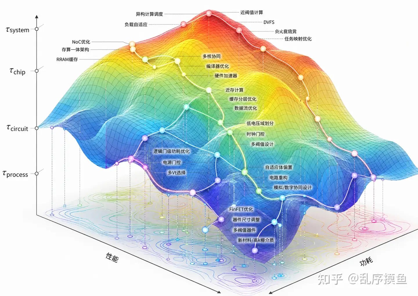
The entire Huawei organization — every worker bee — is optimizing the system’s tau time in their own dimension.
So next, let’s talk about the joint optimization of Kirin and HarmonyOS. That is, the system folding of Tau Law.
Talking about this, some might think the hardest part of logic folding is the process, hybrid bonding, TSV, and 1.5-micron pitch.
These are certainly all difficult. But if we stop at the chip itself, the story isn’t fully told.
Because a mobile SoC isn’t a single chip running bare in a lab. It eventually goes into a phone. Users won’t care how your upper die is folded, how your lower die is connected, or what interconnection pitch you achieved. Users only care about one thing: whether my games are stable, whether photos lag, whether AI responses are fast, whether the phone is hot, and whether battery drains quickly.
So, for logic folding to truly work, it can’t rely on the chip alone to brute-force it. The operating system must be brought in.
This leads to a very important direction: upgrading from Temperature Sensor to Thermal Sensor.
These two terms sound similar, but the thinking behind them is completely different.
Traditional Temperature Sensors are just thermometers. They tell you how hot it is here and there. For example, 80 degrees near the CPU, 75 degrees near the GPU, 60 degrees at the package edge. This information is useful but very limited. It can only tell you ‘how hot a certain point is now,’ but it’s hard to tell you ‘where the heat is coming from, where it’s going, and whether it will get hotter in the next second.’
In the 2D chip era, this kind of point temperature monitoring could barely work. Because heat sources are mostly spread on a plane, though complex, at least it’s like a heat map.
In logic folding, it’s different.
The chip has become three-dimensional. Upper die and lower die are both generating heat. Lower die heat must pass through the bonding interface, dielectric layer, upper die, and packaging material before it can escape. There’s also thermal crosstalk between upper and lower dies. A hotspot might not be directly below the sensor, but its heat is quietly spreading sideways. At this point, looking at just a few temperature points is like judging where a whole building is on fire using only three thermometers at home — definitely not enough.
So what we need is a Thermal Sensor. It’s not a simple thermometer — it’s more like thermal radar inside the chip.
It doesn’t just look at what the temperature is, but also where the heat is coming from, where it’s going, how fast the temperature is rising, how large the temperature difference is between upper and lower dies, what the thermal resistance and thermal capacitance of this region are, and whether there’s a trend of becoming a hotspot in the next few seconds.
Here, thermal resistance can be understood as the resistance heat encounters when moving outward. Thermal capacitance can be understood as this region’s ability to absorb heat. Where thermal resistance is high, heat isn’t easy to dissipate. Where thermal capacitance is small, temperature easily shoots up. Like a room with small windows, poor ventilation, and many people — it’s definitely more likely to be stuffy.
But knowing heat alone isn’t enough. Heat doesn’t appear out of nowhere — heat comes from power consumption. Power consumption isn’t evenly distributed either. It comes from specific modules, specific tasks, and specific power domains.
So there must also be Power Sensors.
What Power Sensors do is tell the system: who is consuming power now, how much, whether voltage is dropping, whether current is surging, whether a certain power domain suddenly burst. Power domains are regions divided by power supply in the chip — for example, CPU, GPU, NPU, ISP, NoC, SRAM, and I/O might each have their own power domain.
If the Thermal Sensor tells you ‘it’s hot here,’ the Power Sensor helps you answer ‘why it’s hot.’ Is the CPU big core running? Is the GPU shader at full load? Is the NPU doing continuous inference? Is the NoC moving data? Is memory access too aggressive? Or is the power network itself losing power?
This is like a doctor diagnosing illness. Only measuring temperature can tell you that you have a fever. But to know whether it’s a virus, bacteria, inflammation, or heatstroke, you must look at more indicators. Chip thermal management is the same — knowing the temperature alone isn’t enough; you must know the heat source.
At this point, the chip side can’t just expose a few temperature registers to the system. It needs a more complete telemetry interface. This interface isn’t necessarily traditional CPU ISA add/subtract/multiply/divide instructions — it’s more like a ‘health reporting protocol’ between the chip and the operating system.
The chip must be able to tell HarmonyOS: how much power the CPU is consuming now, how much the GPU is consuming, how much energy this segment of NPU inference consumed, whether a certain power rail has droop, which region is heating fastest, which hotspot is migrating, and which die layer is thermally crosstalking with another die layer.
Droop is when voltage drops instantly. You can understand it like everyone in a building turning on the faucet at the same time, and the water pressure suddenly drops. When voltage drops in a chip, transistors slow down, timing margin gets eaten, and in severe cases stability is affected.
With this information, what HarmonyOS sees is no longer a few isolated temperature numbers, but a dynamic chip thermal map.
This thermal map isn’t photographed — it’s computed. The chip reports Power Sensor, Thermal Sensor, performance counters, task loads, NoC congestion, memory bandwidth, and power state information. HarmonyOS then combines chip structure models, packaging thermal models, and historical time series to reconstruct a 3D thermal field.
What we want to do is judge ahead of time. Seeing power consumption rising, heat flow direction changing, and dT/dt steepening, we know a hotspot is forming and adjust scheduling ahead of time to suppress the heat. dT/dt is temperature change rate — simply put, how fast the temperature is rising. The temperature hasn’t reached the red line yet, but if it’s rising fast, it’s time to be alert.
So the core of HarmonyOS thermal scheduling isn’t ‘how high is the temperature,’ but continuously asking several questions.
First question: Where is the current hotspot? Is it CPU, GPU, NPU, SRAM, NoC, or upper-lower die thermal crosstalk?
Second question: What’s causing the hotspot? Is it computational power consumption, or memory access power consumption? Is the NoC moving too much data, or is it RF transmission, or is it power network loss?
Third question: How will this hotspot develop? Is it a short burst that will cool down soon, or will it enter sustained heating?
Fourth question: How urgent is the current task? Does the user perceive it? Is there still τ slack?
Here, τ slack can be understood as response time margin. For example, when the user taps a button, whether the system returns in 50 milliseconds or 70 milliseconds, the user might both feel it’s fast. Those 20 milliseconds in between are the margin that can be traded for lower power consumption, lower temperature, and longer battery life. Conversely, if game frame time is already near the threshold, or AI first token is already near the user’s waiting boundary, then you can’t save anymore — you must release performance.
This is τ-DVFS.
Traditional DVFS mainly looks at load and temperature — high load means raise frequency, high temperature means lower frequency. τ-DVFS goes further. It looks at task response time budget. If tasks have margin, lower voltage and frequency slightly, trading τ dividend for lower power consumption and lower temperature rise. If tasks are about to affect experience, release frequency, voltage, and bandwidth to preserve experience.
In plain terms, not all tasks are worth sprinting at full speed. Chip scheduling can’t be like a novice driver, flooring the gas pedal then slamming the brakes. It must be like an experienced driver, knowing when to go fast, when to stay steady, and when to coast to save fuel.
With the thermal map and τ budget, HarmonyOS can do finer scheduling.
For example, a certain NPU region is doing continuous inference. The Power Sensor tells the system that power consumption comes from NPU compute and SRAM access. The Thermal Sensor tells the system that the hotspot is spreading toward the nearby GPU region. At this point HarmonyOS doesn’t necessarily have to brutally chop NPU frequency. It can reduce batch size slightly, stagger some tasks, adjust NoC QoS, limit a segment of memory burst, or delay background AI tasks. The ultimate goal isn’t to suppress temperature to the lowest, but to save heat where users don’t perceive it, and preserve experience where users are sensitive.
Another example is gaming scenarios. The GPU is hot, but the CPU is also hot, and the NPU might still be running super-resolution or frame interpolation. Traditional approaches might just lower GPU frequency when temperature is reached. The result: frames suddenly drop, users curse. The smarter approach is to first judge τ slack and frame time. If frame margin is still sufficient, you can slightly reduce resolution, image quality, or background tasks. If frame time is already near the boundary, prioritize preserving foreground frame rate and push other insensitive tasks back.
Cameras are the same. ISP, NPU, memory, and NoC all participate. The heat source isn’t one point, but a pipeline. If HarmonyOS knows where are sustained heat sources and where are short bursts, it can adjust HDR, noise reduction, and AI algorithm pacing to make the shooting experience stable, rather than dropping frames, lagging preview, and overheating after a few minutes of shooting.
Communication scenarios are even more typical. RF transmission, baseband, CPU, and memory access all stack up, especially in weak signal, video calls, and hotspot sharing. Thermal management can’t just stare at CPU temperature. The system needs to know whether heat is caused by communication power consumption or application processing, then choose different strategies.
Of course, this isn’t easy either.
How to place sensor points in the chip is itself a design problem. Too many, and area and power consumption go up. Too few, and hotspots aren’t accurately seen. Placing next to the CPU can see the CPU; placing next to the NPU can see the NPU. But in 3D stacking, many hotspots transmit between upper and lower dies, and sensors aren’t necessarily right above hotspots. Here, thermal RC models, FEM simulation, packaging boundary conditions, and power consumption profiles must be used repeatedly during the design phase to find a sufficiently effective sensor set.
FEM is finite element simulation — simply put, cutting complex structures into many small pieces and calculating how heat moves piece by piece. Thermal RC models abstract thermal resistance and thermal capacitance into a network, used to estimate the time process of temperature rise and fall.
Runtime isn’t easy either. Sensors have noise, have drift. Different sensor reporting times need to align. Power data and temperature data need to align. Task scheduling and hardware events also need to align. Otherwise the heat you see might already be heat from several milliseconds ago. You think it’s caused by the CPU, but it might actually be residual heat from the NPU’s previous burst.
So what HarmonyOS needs to do isn’t just take data, but establish a lightweight chip thermal digital twin. This term sounds big, but can be simply understood as: the system maintains a real-time shadow map of the chip’s thermal state. The real chip is generating heat, the shadow model follows updates. Sensors calibrate it, power data feeds it, and scheduling results in turn affect the next moment’s thermal state.
What phones fear most is good peaks but bad sustained performance. Product launch benchmarks are high, but games drop frames after ten minutes. AI starts fast, but later token rates jitter. Camera opens smoothly, but continuous shooting overheats. What users perceive isn’t theoretical peak, but sustained stability.
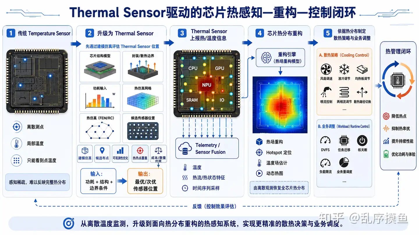
So the goal of this technology stack is to distribute τ dividends well.
Sometimes τ dividends go to performance, letting key tasks complete faster. Sometimes to power consumption, making the phone more battery-efficient. Sometimes to thermal experience, keeping surface temperature down. Sometimes to p95, p99 stability, preventing latency jitter.
p95, p99 are tail latencies. Average values looking good is useless — when the user happens to hit that 1% stutter, they’ll only remember that it stuttered. What system optimization ultimately needs to look at is these real experience boundaries.
So, HarmonyOS thermal perception isn’t just thermal management, but connecting chip, sensors, power supply, packaging, and business scheduling into a closed loop. The chip side is responsible for perception, clearly stating thermal and power states. The system side is responsible for understanding, calculating thermal fields and load trends. The scheduling side is responsible for decisions, redistributing performance, power consumption, heat, and experience. The application side is responsible for cooperation, making trade-offs between image quality, frame rate, model precision, and background tasks.
Of course it’s worth it. Otherwise how could we justify our year-end bonuses?
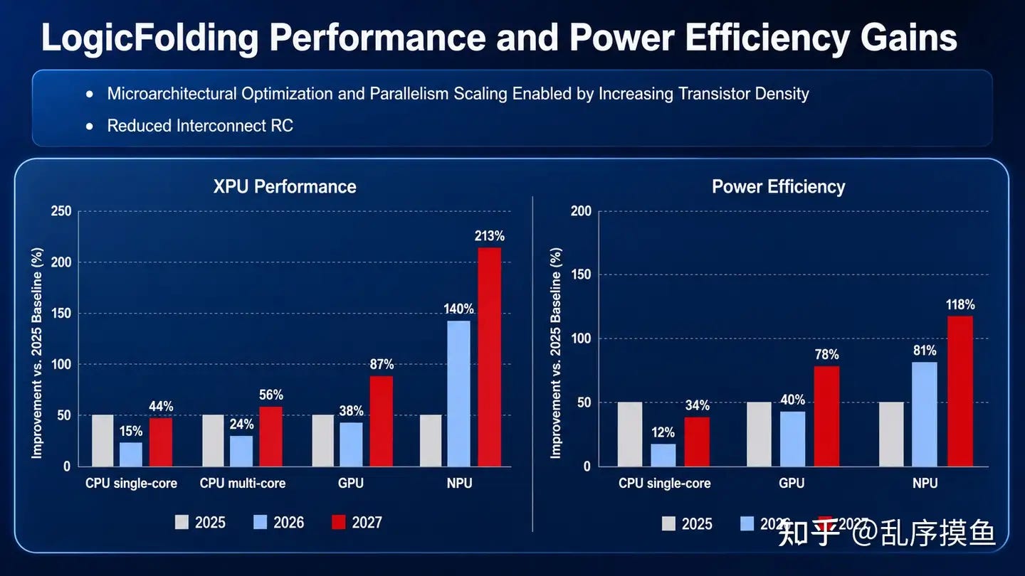
This chart shows the simultaneous amplification effect of LogicFolding on performance growth and power efficiency growth curves. Using 2025 as the baseline, 2026 already shows clear benefits: CPU single-core improvement of 15%, multi-core improvement of 24%, GPU improvement of 38%, while NPU improvement is most significant, reaching 140%.
By 2027, as logic folding further matures, benefits continue to expand: CPU single-core improvement to 44%, multi-core to 56%, GPU to 87%, and NPU to 213% — equivalent to 3.13x the 2025 baseline. Power efficiency shows the same trend: CPU single-core power efficiency improves from 12% in 2026 to 34% in 2027, GPU from 40% to 78%, and NPU from 81% to 118%. This shows that LogicFolding’s value isn’t just ‘stacking more transistors,’ but through higher transistor density, shorter interconnection, lower RC, and better parallelism, simultaneously pulling up both performance improvement and power efficiency improvement. NPU’s growth is the steepest, showing that logic folding is especially suitable for AI computing scenarios with high parallelism, high bandwidth, and high data movement pressure.
Power efficiency benefits also come from these places: shorter interconnection reduces wire capacitance. Lower RC means fewer buffers and repeaters. Shorter clock tree reduces clock power. SRAM and logic being closer means less data movement. Higher vertical interconnection density means more direct local connections. Plus thermal-aware partition can reduce peak power density and improve sustained performance.
Logic folding sounds like a cool technical term, but what it truly proves is not that ‘chips can be stacked.’ The industry has been doing that for a while. What it truly proves is: in mobile terminal SoCs — where space is extremely small, power is extremely sensitive, costs are extremely stringent, and shipment volumes are extremely large — can we truly turn three-dimensional space into design space?
In the past we were accustomed to asking for dividends from process nodes. Transistors get smaller, density gets higher, performance gets stronger, power gets lower. This era certainly hasn’t ended, but it’s getting increasingly expensive and increasingly slow. Today, to keep moving forward, we can’t just ask ‘can transistors get even smaller’ — we must also ask ‘can signals run even closer.’
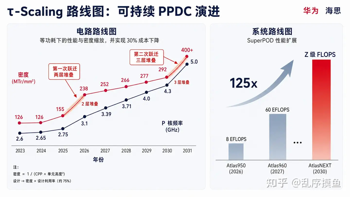
This is the question Tau Law wants to answer.
Tau Law is not anti-Moore’s Law, nor does it replace Moore’s Law. It’s more like finding a new path for system evolution after Moore’s Law slows down: since continuing to shrink on the plane is getting harder and harder, then shorten the time constant τ, fold long interconnections shorter, reduce data movement, and turn signals that originally took long detours on a 2D plane into short-distance direct routes in 3D space.
In plain terms, in the past we mainly drew cities denser on a piece of paper. Now we’re starting to build subways, elevated roads, and 3D transportation. The city is still that city, but the organization has changed.
Mobile terminal SoC practice shows that logic folding can indeed bring higher effective transistor density, and can also bring performance and power benefits. But there’s no magic here. Its PPA (Performance, Power, Area) benefits are highly tied to vertical interconnection density. If hybrid bonding pitch isn’t fine enough, logic can’t be split finely. If TSV, KOZ, heat dissipation, power supply, timing, and yield aren’t handled well, the benefits will be eaten by engineering costs.
So logic folding is not a ‘stacking process,’ but an entire system engineering effort.
It requires mature advanced stacking processes, requires EDA tools to evolve, and requires architecture, RTL, physical design, packaging, process, testing, and system software to coordinate together. EDA is especially critical here. Without 3D-aware, multi-die-aware tool chains, engineers can only probe bit by bit with experience, try round after round with simulation, and change again and again with rework. It can be done, but it’s painful. It can run, but efficiency isn’t high enough. In the future, whoever can deepen the tool chain will be able to release greater PPA potential from logic folding.
This is also very enlightening for China’s semiconductor industry.
We can’t fantasize about solving all problems with a single point technology. Chips aren’t wuxia novels — you won’t pick up a secret manual and suddenly become invincible. True semiconductor capability is built layer by layer: operating system, instruction set, architecture, IP, EDA, materials, equipment, process, packaging, testing, production ramp-up, and application ecosystem.
The significance of logic folding to us isn’t just having another 3D IC route, but reminding us: China’s semiconductor future can’t just stare at ‘catching up on nodes’ — it must also learn to ‘reconstruct systems.’ Nodes must be caught up, tools must be filled in, processes must be polished, packaging must be done, and architecture must also dare to be rethought. Paths others have walked, we need to make up lessons. Paths others haven’t fully walked through, we must also dare to explore.
This path won’t be easy. It’s not corner overtaking — it’s more like rebuilding roads on a steep slope. Corner overtaking sounds exhilarating, but in the engineering world it’s more often climbing: slow, tiring, easy to fall, but as long as the road is built, those who follow can walk more steadily.
Kirin 2026 is not the endpoint — it’s just a node. Its true value isn’t telling everyone ‘we’ve solved everything,’ but proving one thing: when Moore’s Law slows down, the external environment is complex, and mobile terminal space is pressed to the limit, we can still find new evolution directions through system engineering with available processes.
Logic folding is an important practice of Tau Law, and also a feasible, sustainable mobile terminal SoC evolution path. Its core is not stacking chips higher, but bringing signals closer. It’s not filling transistors to the brim, but organizing the system more cleverly. It’s not just pursuing peak performance, but pursuing running fast, running stable, and running long in real phones.