Why would I design my own LoRa board? To recap the last episode, mesh hardware is living in the past. The most popular LoRa chip, the SX1262, is over 8 years old. There have been two generations of new LoRa chips released since the SX1262, and yet manufacturers keep using it in new designs. So I decided to design my own hardware using the latest and greatest Semtech chip, the LR2021. Click below if you want to read more about why I think you too should be excited about shiny new things:1

So what exactly is involved in designing a LoRa board? If this sounds like a wild idea, let me demystify it a bit.
Whether you’re using a RAK or Heltec or Seeed, all these boards consist of essentially two components: an MCU and a LoRa chip. The most common choices are probably the NRF52840 and the SX1262. Connect these two things together and you basically have yourself a mesh node. Some manufacturers will add a GPS module, or a FEM, or a filter, but they’re all basically dressing up the same core components. Most of the complexity has been pushed into the chips themselves. I am not a traditionally trained electrical engineer, but this seems to be a common pattern. More and more of the complexity of modern circuits has moved into chips, and you can get quite far just gluing these Lego blocks together. Designing the entire RF chain for a radio sounds hard! But luckily, I don’t have to. Semtech’s LoRa chip does most of that for me. I just have to send it commands over the SPI bus.
Most of my professional experience has been in software, but I think there are parallels to draw here. The traditional route to software is to spend 4 years on a degree learning about algorithms, data structures, and how compilers work. Then you get your first job and realize all the algorithms, data structures, and compilers are already implemented. So I hope you like gluing web frameworks together! For a new grad, it can be a pretty disillusioning realization that most software engineers aren’t implementing red-black trees. One guy did that 20 years ago, and posted it for free on the internet. So get back to work, kid! Those React components aren’t going to write themselves (well, in the age of AI, maybe they will).
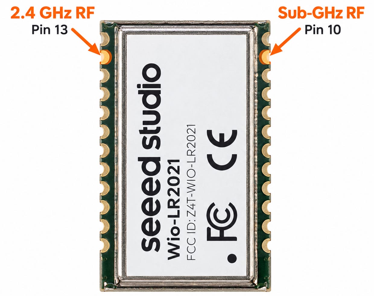
So anyway, to create my LoRa board, I basically just need to glue one of these Wio-LR2021 modules to a XIAO postage-stamp MCU module.
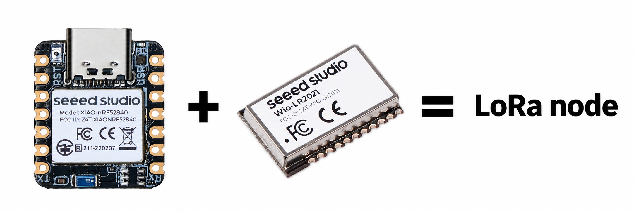
That should be just a matter of designing a PCB that runs a few data lines between the two components. How hard could it be?
So I pop open KiCad, and draw a few data lines. These data lines are low speed and so anything halfway reasonable will likely work just fine. The hardest part about this process is probably hunting down the footprints for the Wio and XIAO modules. I send it off to JLCPCB and this arrives in the mail a couple weeks later.
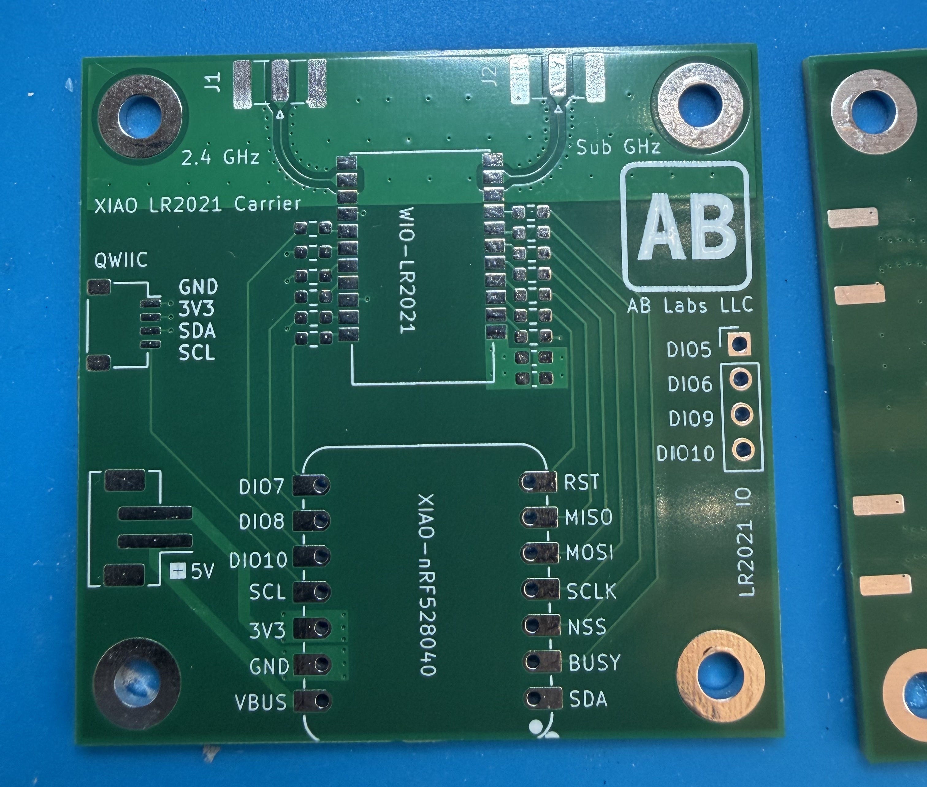
Beauty!
I spend an hour with a solder paste stencil and some tweezers…
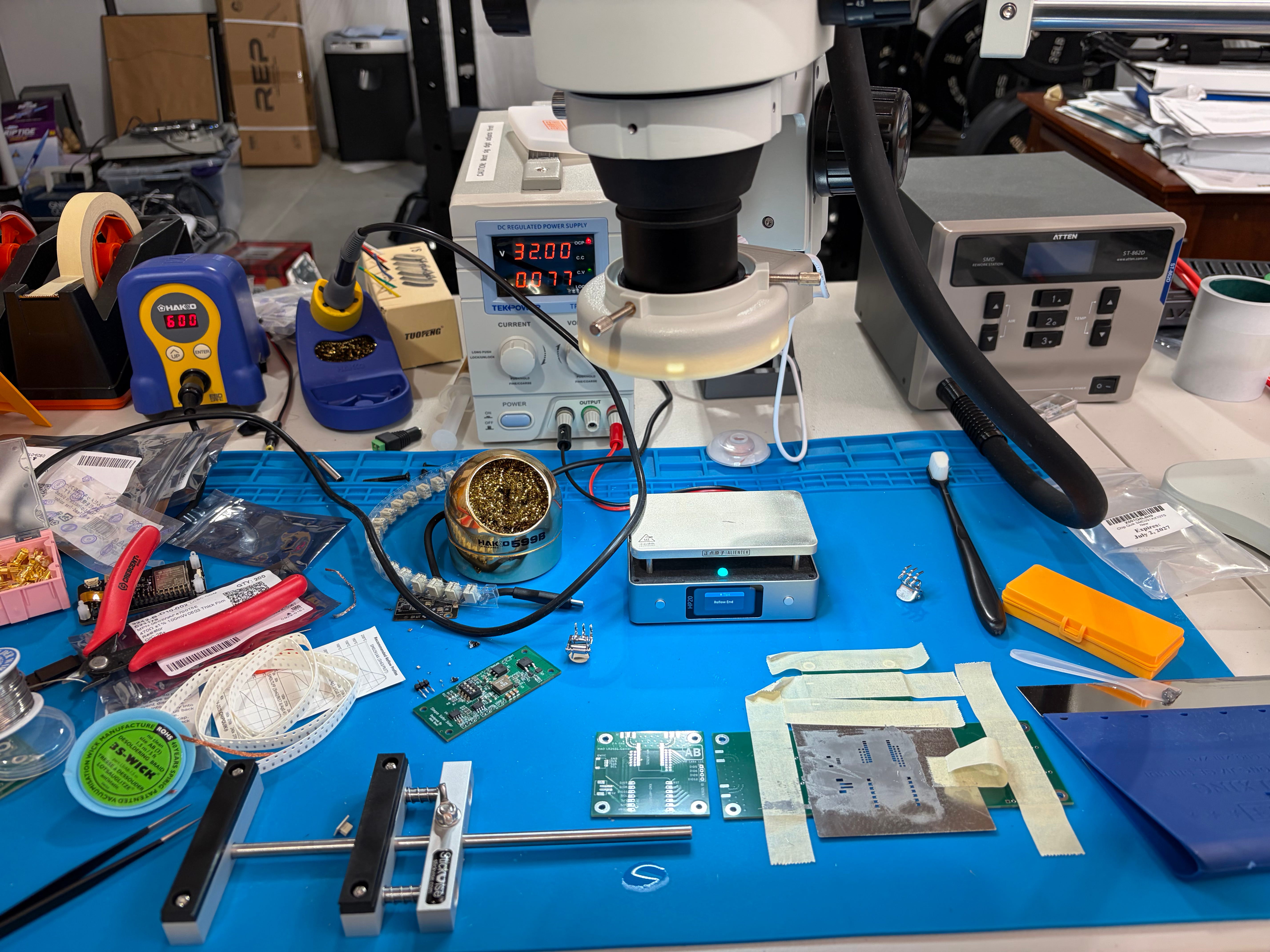
And then I solder it all together with my hotplate.
And there it is, the physical manifestation of my design. Naturally, I attach it to the custom solar power supply I designed and I’m sending messages to my local mesh.
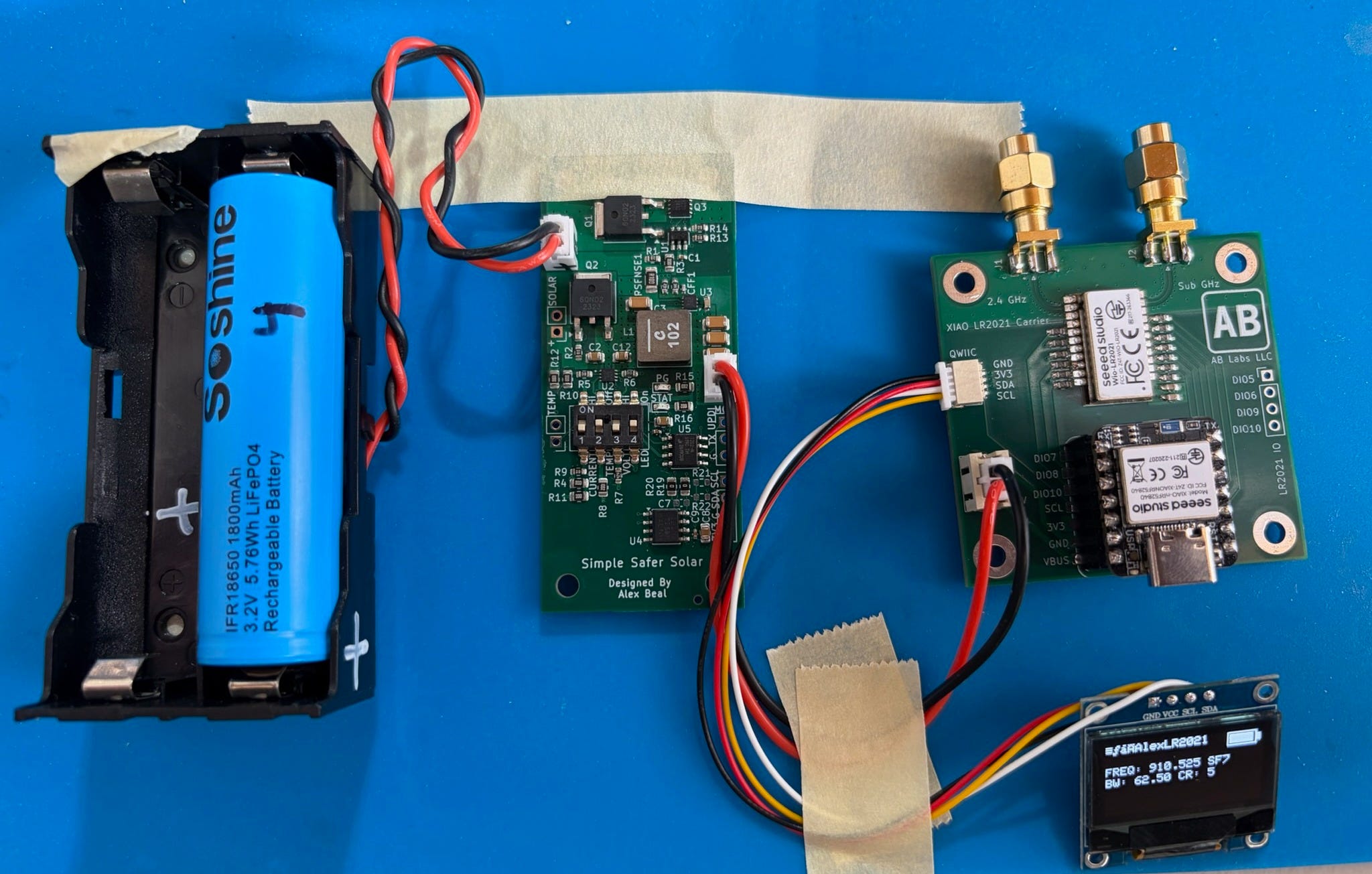
Easy-peasy lemon squeezy! Just a couple data lines, right?
So I left out one tiny detail. Sure, connecting the XIAO to the Wio is just a couple data lines, but what about the RF signal? The Wio module doesn’t have any onboard IPEX connectors, it only has a couple pads. So I need traces on my board to get the RF signals from the Wio’s pads to some sort of antenna connector. As you can see from the pictures above, I opted for edge mounted SMA ports.
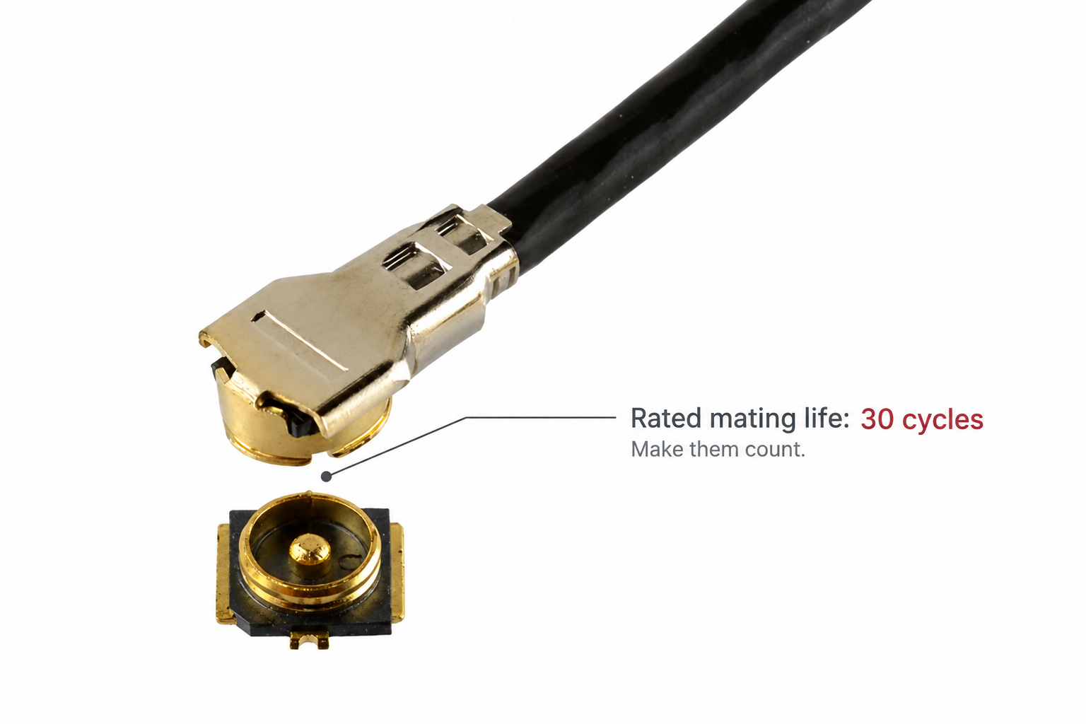
I probably could have made my life easier if I had just plopped down a couple IPEX connectors next to the module, but honestly I hate those things. Did you know IPEX connectors are only rated for 30 insertions? Yeah, that’s not a typo: 30 insertions. Make them count!
So instead of a couple surface mount IPEX connectors, I’m going to do this in a way that requires maximum effort. I’m going to run the RF signal from the Wio’s pads to the edge of the board.
What makes this difficult? Impedance matching. You don’t have to spend much time with radios before you learn that bird is the word and 50 ohms is the magic number. Most folks are familiar with this concept when it comes to antennas. The antenna itself must be 50 ohms. If it’s not, the signal will be reflected back at your transmitter potentially damaging it. Usually at this point, everyone nods and the explanation stops there. But in order to understand why this antenna trace gave me so much trouble, we need to go deeper.
What exactly is an impedance? Well, from the unit, “ohms”, we can guess it’s something like resistance, but with a little more RF magic sprinkled on top. So let’s start with resistance. We often think of it as something that resists the flow of electricity. Electricity doesn’t flow very well through something with high resistance, and flows more easily through something with low resistance.
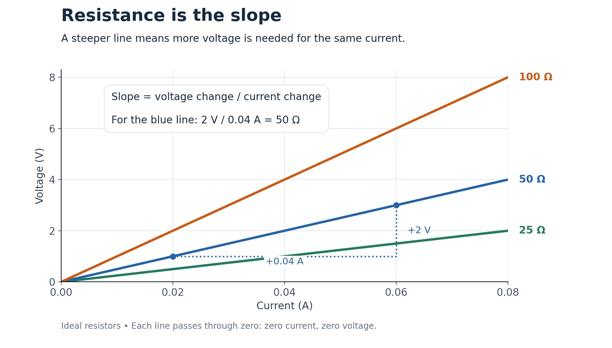
But I think a more abstract way of thinking about resistance is that it’s just the quantity that tells us the relationship between current and voltage. When we apply a voltage to a resistor, it’s the resistance that tells us how much current we can expect to flow. If we graph voltage versus current, the resistance is the slope of the line. It uniquely identifies that voltage-to-current ratio.
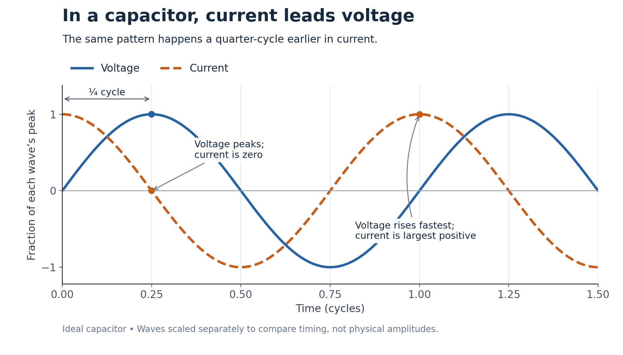
So far so good. But things start to get weird as soon as our voltages begin to vary over time, like, for example, when we start working with RF signals. A 915 MHz signal is cycling between positive and negative 915 million times per second. Now we can no longer always describe the relationship between voltage and current with a single number. Why? If voltage is a sine wave, then, in a linear circuit, current will also be a sine wave and those two sine waves may not be perfectly synchronized. A capacitor is the classic example. If we apply a sine wave voltage to it, as the voltage is increasing fastest, current will rush into the capacitor, but at the instant the voltage reaches its peak, current will momentarily be zero. If we graph this out, we’ll see that voltage lags behind current.
So to describe that relationship, we need two quantities: first we need something that describes the magnitude of the relationship. Are the current and voltage waves equally large, or is one larger than the other and by how much? And then we need a quantity that describes how much the current is either lagging or leading the voltage. This is the phase of the relationship. Below, you can see these two concepts broken apart. The first row shows different magnitude relationships, and the second row shows different phase relationships.
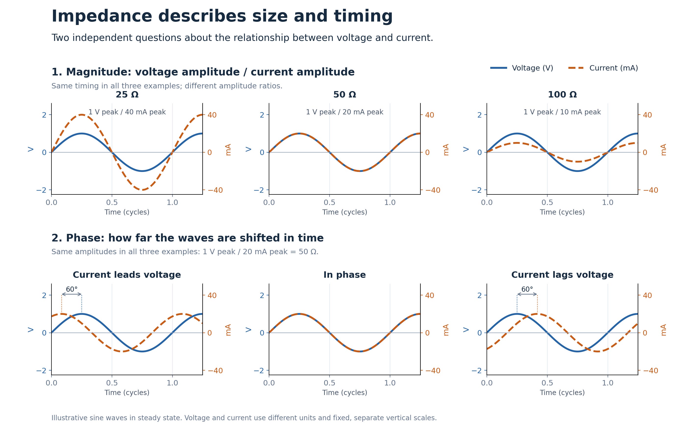
Magnitude has a unit of “ohms” just like resistance, and phase is described in degrees, because circles.2 Now we can understand “50 ohms” in the context of antennas as “50 ohms and 0 degrees”. Conversationally, we drop the degrees since they are zero. Also, I don’t want to go too deeply into this, but know that impedance is often described in terms of a complex number, like 75 + j10 ohms. This is just another way of conveying the exact same information in a different form.3
Whew boy ok let’s get back to the problem at hand: impedance matching. We now know enough about impedance to develop an intuition for why an impedance mismatch causes a reflection. Impedance tells us the relationship between voltage and current. A 50 ohm antenna requires the voltage and current at the connector to be in phase (0 degrees), with 50 volts for every amp of current (50 ohms). Meanwhile, a wave traveling down 50 ohm coax already has that relationship. When the wave reaches the antenna, it delivers its power without a reflection. Success!
But suppose the antenna is 100 ohms instead. The incoming wave still has the voltage-to-current ratio set by the 50 ohm coax, but the antenna requires a different one. It expects the voltage to be 100x the current instead of 50x. So what happens?
Well, a reflection happens! But why? As a first approximation, the intuition is that the incoming signal has the wrong voltage-to-current ratio for the antenna to absorb. So since the 100 ohm antenna can’t fully absorb the 50 ohm signal coming down the coax, some of that signal gets sent packing back toward the transmitter.
To refine this understanding a bit, what we need to know is that when the wave reflects, it actually combines with the incoming wave. That combination will form a new voltage-to-current ratio at the connector. It’s this wave that will, at the connector, turn out to have a 100 ohm voltage-to-current ratio. In other words, the antenna will reflect just the right amount of current and voltage such that the antenna’s 100 ohm requirement is satisfied.
And now we can finally understand this antenna trace on my circuit board: First, just like every other part of the signal path, it must be 50 ohms. Second, to make it 50 ohms, the trace must have a certain geometry, and that geometry is a function of the materials used to make the PCB.
What this means concretely is you go to your PCB manufacturer’s website and look for an impedance calculator. You plug in all the numbers, and it will say: for your board, a 50 ohm trace should be 0.14 mm wide. Then in KiCad you set the trace width to 0.14 mm and everything just works, right?
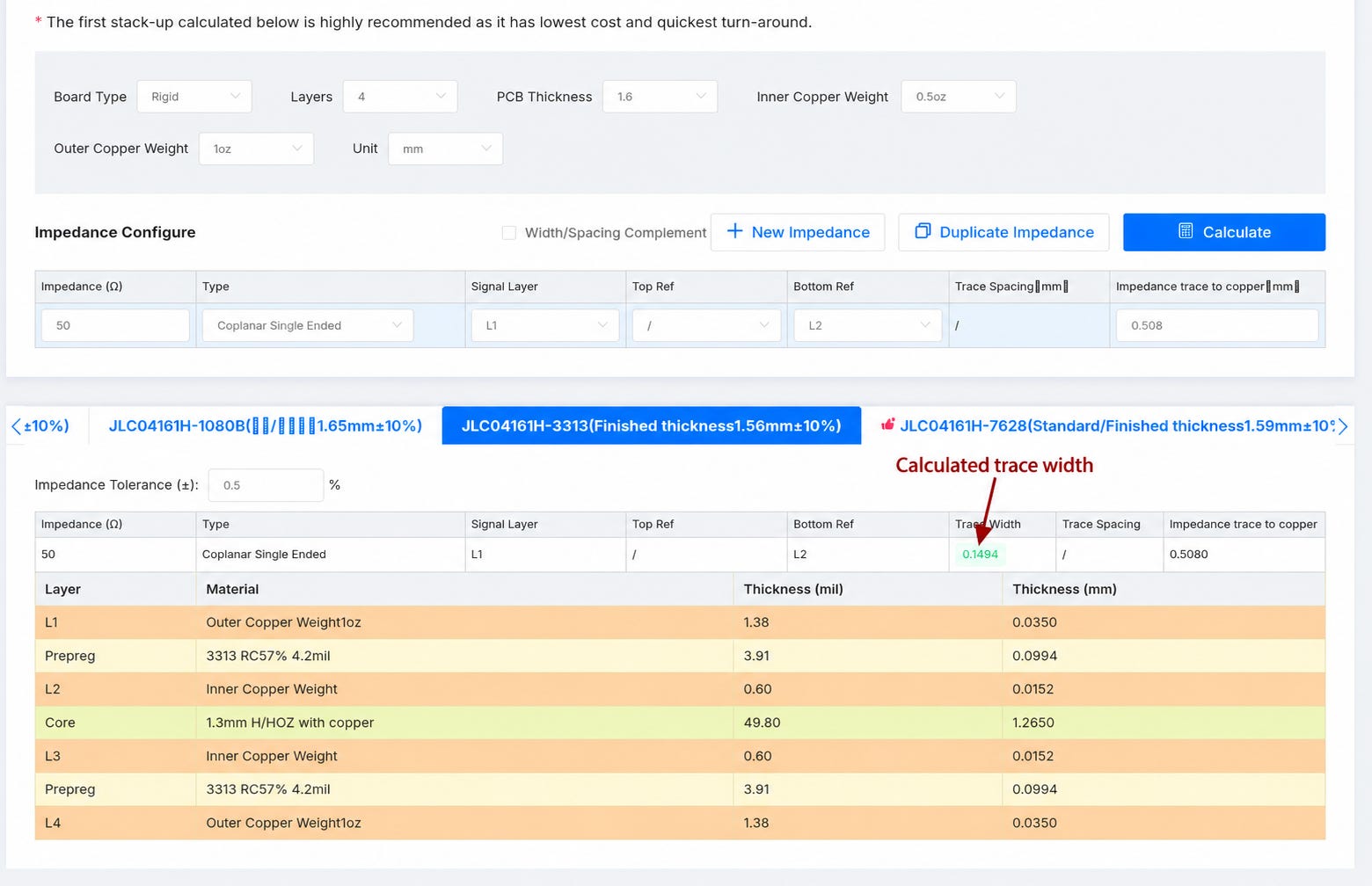
Unfortunately not for me. Here’s what the trace looked like in KiCad:
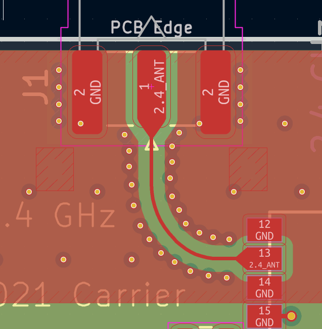
And looking at it, you can see it kind of resembles a cross section of a coax. That’s no coincidence! That same geometry that makes a coaxial cable work translates over to the PCB.
So then why didn’t it work?
To test this trace, I connected the SMA connector to my VNA via a short length of coax and added 50 ohms of resistance at the pad meant for the Wio module.
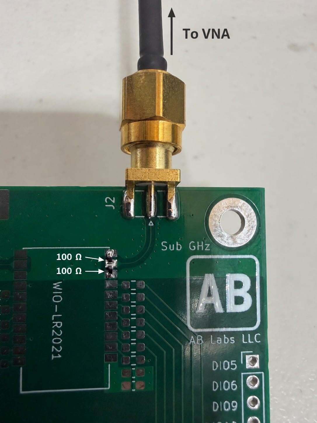
What my VNA does is it sweeps from 9 kHz to 3.2 GHz and tells me the magnitude of the reflected signal at each of those frequencies. If the trace and connector are 50 ohms, the resistors should absorb basically all of the signal, and the reflected signal should be tiny, say, less than -20 dB. If something along the signal path is not 50 ohms, I’ll see a larger reflection.
So what did I get? Survey says:
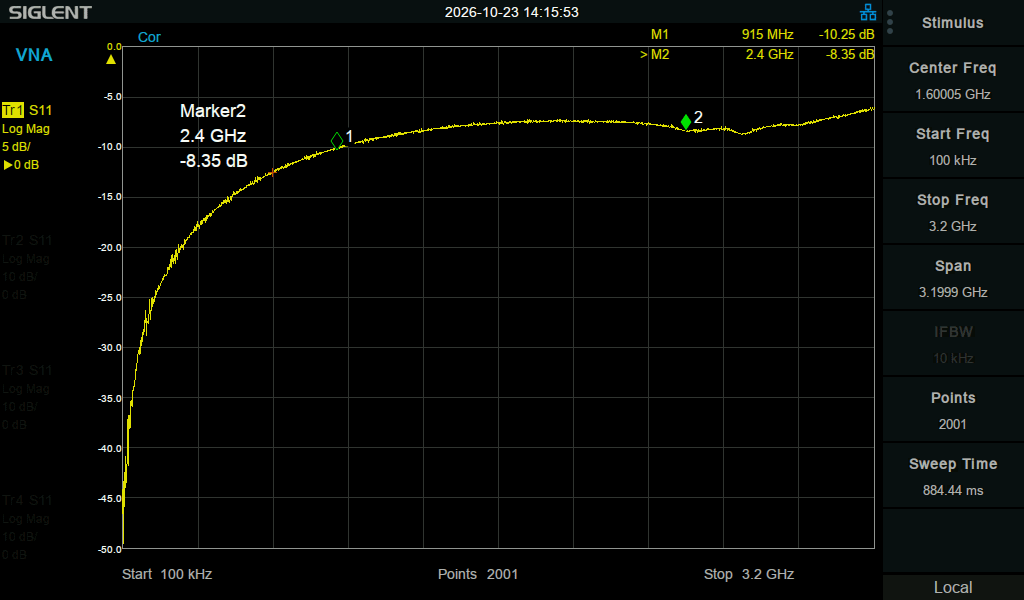
So I got -10 dB on 915 MHz and -8 dB on 2.4 GHz. I’d roughly translate this result as, “Nice try, sport. Next time, leave the RF to someone who knows what they’re doing.”
So what does one do in this situation, other than leaving it to someone who knows what they’re doing? Well I double checked JLC’s impedance calculator and was pretty confident my traces were correct. So my attention turned to the pads for the SMA connector.
If the pad or connector was the issue, I should see a much better result if most of the pad were removed. So under a microscope, I used an x-acto knife to remove most of the pad, and tacked a coax cable onto the tiny bit of pad I left behind. It’s hard to see, but under that coax, most of the center pad is gone.
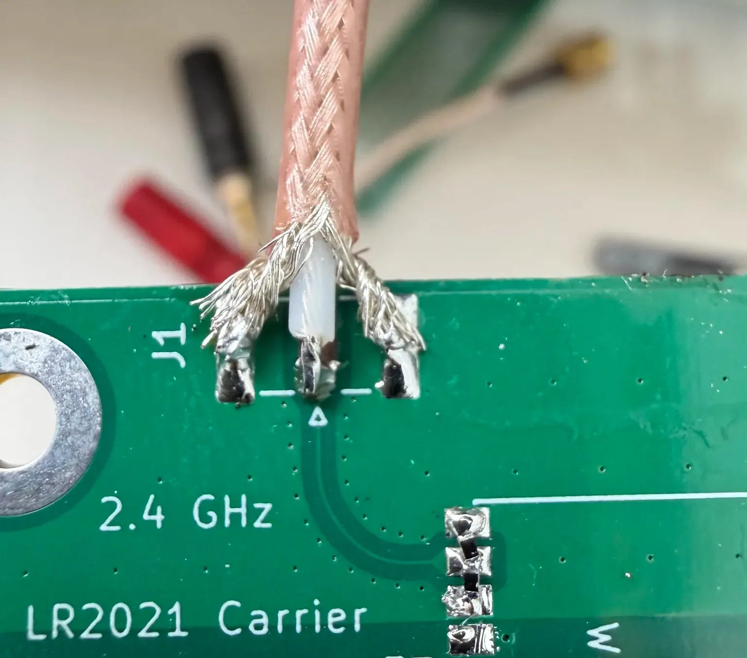
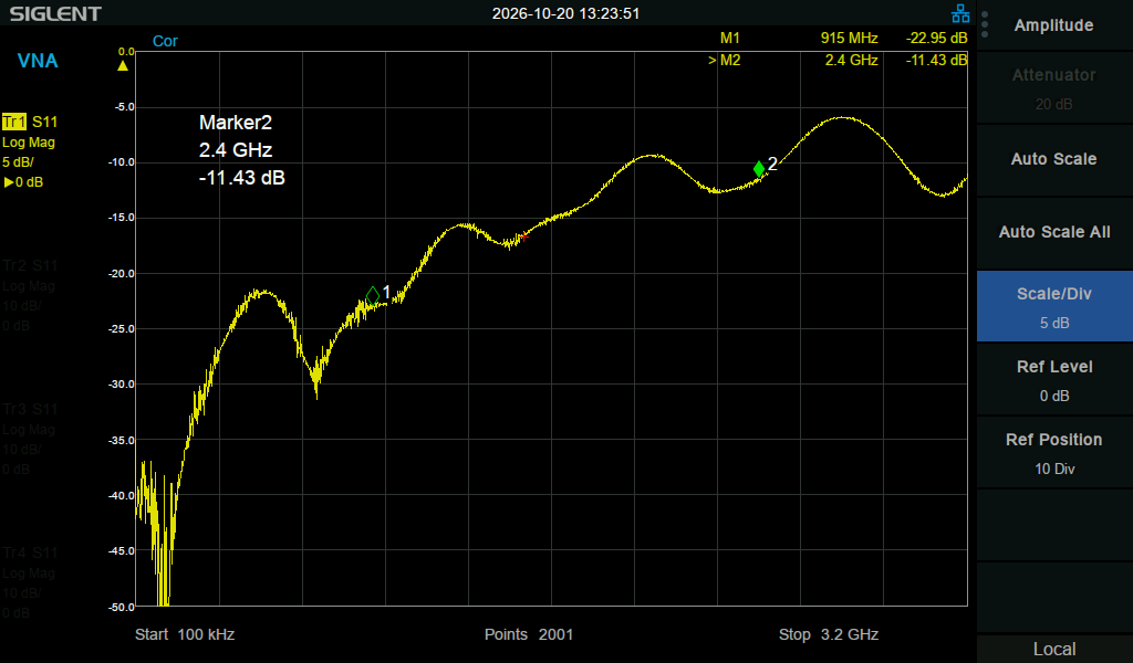
I reconnect it to my VNA and lo and behold, I see a dramatic improvement at 915 MHz and a pretty good improvement at 2.4 GHz. -22 dB and -11 dB respectively.
Ok so what’s wrong with the pad?
I do a few more experiments. My most successful one is shaving literal fractions of a millimeter off each side of the pad and then soldering the SMA connector onto what remains. My theory is that if the trace needs to be tiny (0.149 mm) to have an impedance of 50 ohms, perhaps the pad is just way too wide. This experiment works and gets both frequencies down to about -15 dB. Not perfect, but I could live with that (with a bit of shame perhaps).
So should I just thin out the pad and send it? No, we must go deeper.
So just taking a step back for a moment, I want to highlight something: this is crazy right? Tenths of a millimeter on your pad can have a huge effect on your signal integrity.
This is why RF is widely believed to be a branch of the dark arts. I think the main reason for this is that everything affects everything else. In software, when changing one thing ends up breaking something seemingly far away, we say that the system is highly coupled. This is widely considered to be bad.
To me, RF seems to have this problem. You can draw out a perfectly sensible schematic, but if the pad on your SMA connector is 0.2 mm too wide, the whole thing falls apart. It’s madness!
I think nothing drives this point home better than learning about how RF engineers have resorted to simulating electromagnetic fields over their entire boards. Everything is so highly coupled, that the best way to understand what the hell is going on is to draw the physical manifestation of your circuit in CAD and then simulate literal EM waves propagating over the entire device. So much for Ohm’s law, we’re just going to solve Maxwell’s equations instead.
Anyway, so that’s what I did.
In the video above, you can see my antenna trace on the left, and you can see colors corresponding to the vertical electric field. That’s how a pulse propagates down the trace.
Does the simulation actually work? Yes, it matches my VNA measurements almost perfectly. In the graph below, you can see a solid black line and a solid grey line. The black line is the magnitude of the reflections measured on my VNA, and the grey line is the model’s prediction. They overlap almost entirely. Incredible.
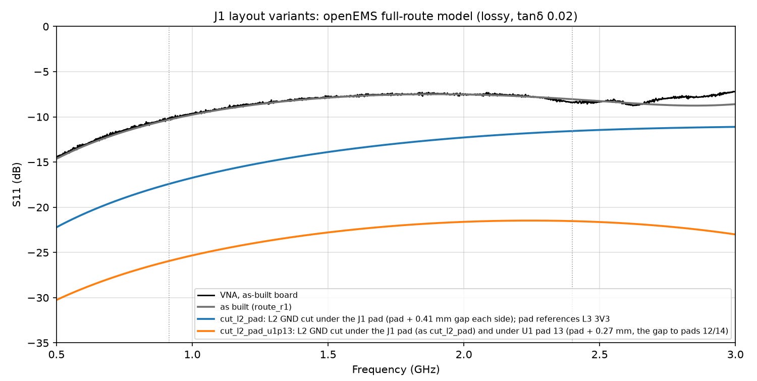
And the blue and orange lines are two possible modifications that, in the simulation, reduce the magnitude of the reflections by quite a bit. They involve removing the copper on the layer below the pad, which happens to be a ground plane (literally a plane of copper connected to ground). The intuition is that at these frequencies, the pad is acting as a capacitor, and by removing that ground plane, it greatly reduces the capacitance and gets me closer to 50 ohms. Voodoo.
And for now this is where the story ends. The next step is to decide which route I want to go. I could try removing the ground plane below the connector. Another idea is I could change the stackup of the board, increasing the distance between the signal trace and the ground plane below, so that the 50 ohm trace is wider. That would make the difference in width between the trace and the pad smaller, and hopefully bring the pad closer to 50 ohms.
If you’ve stuck with me this far, thank you! And if you’d like to know if I actually manage to fix this board, or if I’d be better off leaving RF to the professionals, go ahead and smash that subscribe button. Now go out there and make some (EM) waves.