I wouldn’t call the semiconductor industry a “system” in the organic sense, but it is undeniable that it has become a critical fabric of our society. Everything relies on them: from your computer, your phone and your car, to your toaster, and your kids’ toys. Not all the semiconductors are manufactured equally, or require the same kind of advanced technology, but they are all needed one way or another.
Much of what I am going to write about in this post have probably been covered to a large extent by SemiAnalysis, the leading research company “specialised in the Semiconductor and AI industries” (if you like semiconductors and AI I highly recommend giving them a read and subscribing, they create really high-quality content).
However, I felt the need to write this high-level overview as a learning exercise to myself, at the risk of repeating something that is common knowledge. This urge was triggered after reading this article from the Japan Times that describes “How China built its ‘Manhattan Project’ to rival the West in AI chips” by creating their first prototype of extreme ultraviolet lithography machine (EUV). This was achieved by reverse-engineering ASML’s EUVs designs, completely shaking the geopolitical board. A board where we were used (and quite comfortable) relying on a small number of companies to manufacture the world’s advanced semiconductors. Unfortunately, this scenario may be coming to an end. Let me show you why.
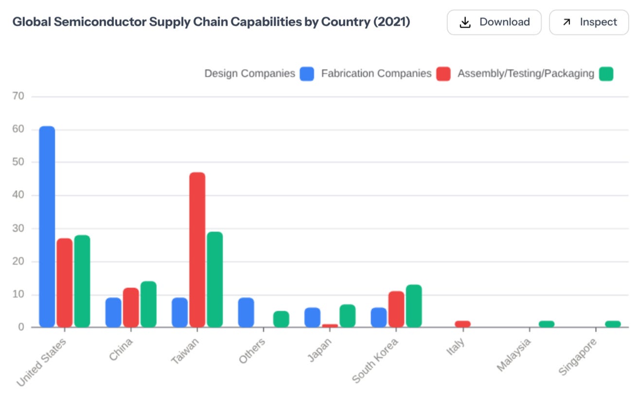
Unlike the food supply chain (see last week’s post), which is often decentralized (where anyone with land can grow wheat), the semiconductors supply chain is defined by extreme concentration end-to-end. The barriers of entry are so high that only two or three companies in the world matter at each stage of the value chain. Let’s do a rundown of the participants of today’s machine:
These entities are the ones responsible for designing the chips that we use on our day-to-day devices. They are all generally “Fabless” Designers, i.e. they own zero factories. What they do is create digital blueprints of their chips that they send to the companies that run the fabrics which are the ones actually making the chips. Examples or architects are companies like Nvidia (of course), AMD or Qualcomm.
Their dominance isn’t built on manufacturing prowess, they leverage their ecosystems and IP as their moat. For instance, Nvidia’s stranglehold on AI doesn’t come just from the chip itself, but from CUDA, a proprietary software language that millions of developers have spent 15 years mastering and optimising their workloads to target. Switching away from Nvidia isn’t just a matter of buying a cheaper chip from AMD, it may require rewriting entire code bases, and re-architecting many of the existing optimisations to target the new chips and new languages. Fortunately (maybe?), Nvidia’s CUDA monopoly may be slowly breaking with the big players like Google and Amazon building their own accelerator chips (TPUs and Trainium)..
Not all chip makers are Fabless or AI-specific, there are also Integrated Device Manufacturers (IDMs) like Intel, Samsung and Texas Instruments that design and build their own chips (owning massive factories with their corresponding OPEX), and other “Fab-lite” companies like Infineon, NXP, STMicro, and Renesas. This is why the supply chain is so messy. NVIDIA (Fabless) relies 100% on TSMC. But a car company (like Ford) relies on IDMs (like NXP) who partially rely on TSMC. If TSMC breaks, everyone feels it, even the IDMs. But more on TSMC in a minute.
Building a transistor is a hard physics problem and as such, you need tools that operate at the edge of physics. This is the domain of the toolmakers, which includes companies like Applied Materials, Lam Research, and the industry’s beast that you’ve probably heard of already, ASML.
This sector is the hidden chokepoint of the global economy. ASML, based in the Netherlands, is the sole supplier of Extreme Ultraviolet (EUV) lithography machines. These devices cost over $200 million each and use light to “print” the most advanced chips.
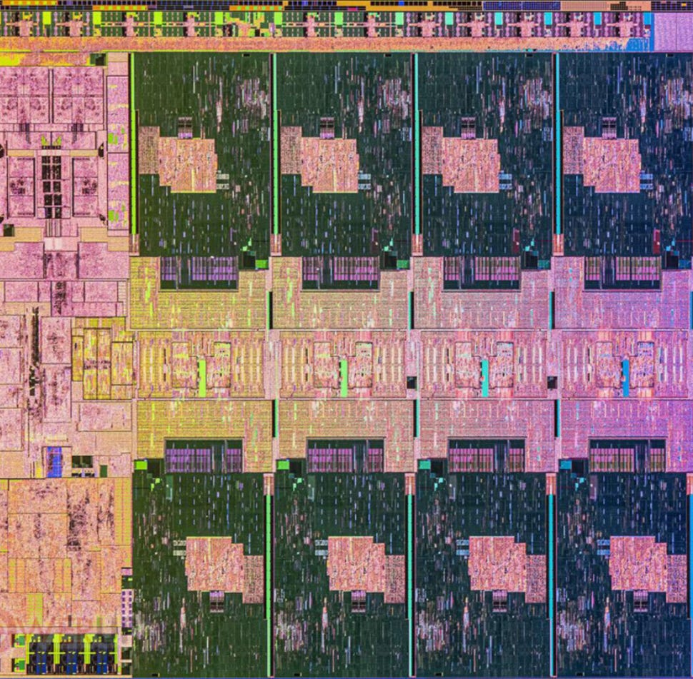
To understand why these machines are so expensive, let’s describe briefly how they work. Fabricating a chip is essentially photography at an atomic scale (as depicted in the RX image of a chip’s blueprint below).
You start with a pure silicon wafer, coated in a light-sensitive chemical called “photoresist.”
Inside the ASML machine, a droplet of tin is hit by a high-power laser twice in rapid succession, vaporizing it into plasma that emits a specific wavelength of invisible EUV light.
This light is bounced off a series of mirrors (lenses absorb this light, so they cannot be used) and directed through a “mask”—essentially a blueprint of the chip’s circuitry.
The pattern is projected onto the wafer. Wherever the light hits, the chemical structure of the coating changes.
The wafer is then washed in acid. The parts exposed to light wash away, leaving behind the physical pattern of the circuit. This process is repeated up to a hundred times, layer by layer, to build a 3D map of transistors as the one below.
The moat here is sheer complexity. ASML’s machines are likely the most precise instruments ever built by humans. They rely on mirrors from Carl Zeiss in Germany that are so flat that if you expanded them to the size of the Earth, the largest bump would be less than a millimeter high.
This is why China’s attempt to reverse-engineer the machine is so difficult. They might be able to steal the blueprints, but replicating a supply chain that requires the world’s best lasers (Cymer), the world’s best glass (Zeiss), and the world’s best system integration is a task that has, so far, defied even the resources of a superpower.
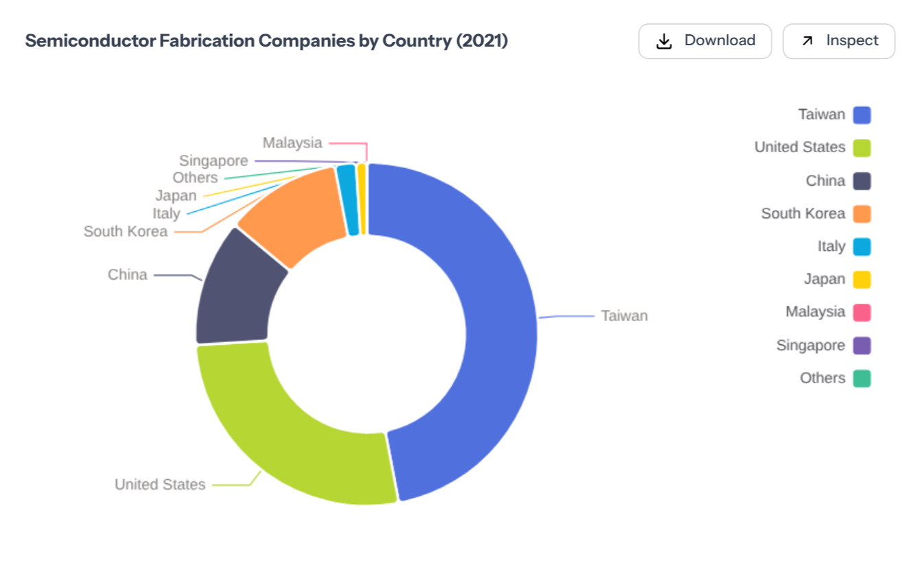
These are the companies responsible for running the fabrics that actually make the chips. Here we find the renowned TMSC (Taiwan) along with others like Samsung (Korea) and Intel (USA). The barrier to entry here is financial and operational terror. Building a single leading-edge Fab costs between $20 and $30 billion (as we are seeing more now with a lot of these companies moving their operation to US soil), making it one of the most capital intensive infrastructure projects (along with maybe data centers).
If for instance a startup tried to print a wafer of sophisticated chips, 90% might come out broken. When TSMC does it, 90% comes out perfect. Tweaking temperature, pressure, and chemistry in real-time is a hard engineering problem that requires experience. This execution gap is why TSMC effectively holds a monopoly on the world’s advanced AI chips.
A modern fab is essentially a cash incinerator that only turns a profit if it runs at nearly 100% capacity (i.e. 24/7/365). The fixed costs, depreciation on $200M machines, massive electricity bills, and ultra-pure water systems, are astronomical. If demand drops and the fab runs at only 70% capacity, the company bleeds billions. Because a fab takes 3-5 years to build and calibrate, companies must bet their entire balance sheet on what the world will want five years from now. If they under-build, they lose the market. If they over-build, they go bankrupt. This is why companies like AMD became fabless in 2008, and IMDs like Intel are bleeding out.
Once a chip is printed, it is fragile and useless. It must be cut, tested, and encased in the black plastic shell you see assembled. This is the role of Packaging and Testing firms like ASE and Amkor.
Historically, this was the boring low-margin part of the supply chain, often offshored to cheaper labor markets. But with the rise of AI and more advanced semiconductors, packaging has become the primary bottleneck. We have hit a physical limit on how big we can make a single chip, so the industry has shifted to “Advanced Packaging” (specifically a technique called CoWoS).
This involves stitching multiple smaller chips (”chiplets”) and high-bandwidth memory blocks together like 3D Lego bricks. It is an incredibly delicate process. Right now, one of the shortages of AI chips isn’t necessarily due to a lack of silicon, but due to a lack of capacity to package them together. This last mile is effectively determining the speed of the global AI rollout, transforming what was once a commodity service into a critical strategic asset. I highly recommend this series on Advanced Packaging from SemiAnalysis to understand why and how packaging is evolving and becoming a new bottleneck for the industry.
If the story ended with the manufacturers, we would be missing the most disruptive shift in the last decade. For forty years, Intel and Nvidia built the engines, and computer companies integrated them into devices. But recently, the biggest customers, mainly Apple, Google, Microsoft, Amazon, Tesla realised that general-purpose engines weren’t enough, and they started building their own chips and integrating them directly on their systems. This is the rise of the Integrators.
Apple led the change in an attempt to solve a bottleneck that had plagued consumer computers for decades: copying between different memory pools. In a traditional PC, the CPU and the GPU have separate pools of memory. To collaborate, they have to constantly copy data back and forth, wasting time and energy. Apple’s solution, the Unified Memory Architecture (UMA) found in their M-series chips, physically merged these pools. This is why a MacBook Air can run local Large Language Models (LLMs) faster than a massive desktop rig, it doesn’t waste time copying data. In the process, Apple managed to generate a new potential moat in the co-design of hw/sw on their devices (removing its reliance on companies like Intel).
On the other side we have Google and Amazon that realised that buying Nvidia’s general-purpose GPUs for every task was expensive and in many cases an overkill. Hence, they began building accelerators for their specific tasks by creating their own ASICs (and this is how Trition and TPUs were born).
This specialization forced them to redesign the entire data center around the chip. Google, for instance, couldn’t just plug these chips in with standard cables. They had to invent Optical Circuit Switches (OCS), using tiny mirrors and beams of light to move data between server racks because copper wires simply weren’t fast enough. This also opened for them the door for less dependency on big architects like Nvidia, while improving their local workloads.
If you look at the semiconductor supply chain from a distance, it looks like a global web. But if you look closer, it looks much more like a funnel. A great way to understand the current state of affairs, and how companies like Apple have found themselves in this situation, is to read Apple In China from Patrick McGee. I read it this summer completely by chance and I can’t recommend it enough.
For fifty years following Moore’s Law, the mandate has been to double the number of transistors on a chip every two years. In the early days, this was a difficult engineering challenge. Today, it is a physics-defying, capital-incinerating nightmare.
As we pushed the boundaries of physics by making smaller and smaller semiconductors, the cost of staying in the game skyrocketed. Building a leading-edge fab didn’t just get more expensive, the costs grew exponentially as we described above. The R&D burden to make the next leap in miniaturization requires pouring billions into research before you sell a single chip, while a modern fab costs $20 billion. To justify that investment, you need massive volume.
This economic pressure created a “survive or die” environment. Companies realized they could not be generalists. They could not be “pretty good” at five different steps of the manufacturing process. To keep up, they had to pour every cent of capital and every ounce of engineering talent into one specific slice of the stack.
As the complexity of chipmaking increased, the number of companies capable of competing at the cutting edge collapsed. In the 1990s, there were dozens of companies competing to build lithography tools. But as the wavelength of light needed to print chips moved from deep ultraviolet to extreme ultraviolet (EUV), the difficulty ramped up. One by one, competitors dropped out. They couldn’t justify the R&D spend. They couldn’t solve the physics, and there is not enough talent to serve them all.
The result is an interdependent chain of monopolies and duopolies. We have created a world where the entire digital economy rests on single points of failure: ASML owning the lithography monopoly with a 100% of the market share, and TSMC with the manufacturing monopoly with close to a 90% of advanced chip manufacturing share.
And as it happened with the food supply chain, by engineering one of the most efficient and advanced manufacturing processes in human history, we also introduced extreme fragility. There is no backup plan. A fragility that is being leveraged geopolitically by the big super powers of the world.
Our dependency on semiconductors, and the extreme concentration of its value chain is being seen by governments as a weapon. I would mark the turning point on October 7, 2022. This was the day the United States effectively declared economic war on China’s technology sector.
The US Department of Commerce didn’t just issue a few sanctions, they weaponized the bottlenecks identified in the previous section. They looked at the semiconductor stack and realised that while China was huge, it was missing the hardest-to-replicate links in the chain. You can’t design a modern chip without Electronic Design Automation (EDA) software, so the US cut off access to them. You can’t print a leading-edge chip without ASML’s EUV machines so the US pressured the Netherlands to ban exports. You can’t train a leading-edge AI model without NVIDIA’s GPUs (at least then, as this is slowly changing), so the US banned the sale of the most powerful chips.
China, realizing it was being squeezed out of the future, looked for its own chokepoints. While the West obsessed over the top of the value chain (design and lithography), China had quietly cornered the bottom in the processing of materials. Mainly gallium and germanium, which are essential for radar, radio communication, and advanced electronics, with China refining 98% of the world’s gallium and more than 60% of its germanium. China also dominates the processing of graphite and other materials that are essential for EV batteries.
Even more, while the US controls the technology, China controls the customer. To understand this counter-leverage, one must look at the thesis presented in Patrick McGee’s book mentioned above.
McGee argues that Apple didn’t just “hire” China to build iPhones; it effectively trained an entire nation in advanced manufacturing. For twenty years, Apple transferred blueprints, equipment, and engineering expertise to Chinese suppliers to build the most efficient supply chain in history to maximise its margins. That efficiency is now a prison. With around 95% of iPhones still assembled in China (even with the latest attempts to minimise the dependency) and nearly 20% of its revenue coming from Chinese consumers.
This gives Beijing a powerful “kill switch.” By banning iPhones in government agencies (as seen in 2023) or launching “tax audits” on Foxconn, China can crash Apple’s stock price and send shockwaves through the US economy. It acts as a massive “corporate shield,” forcing the US to tread carefully lest they accidentally detonate their own flagship company.
So the conflict is served!
What we are witnessing now is what I like to call “the death of the global chip”. Companies and nations were collaborating and specialising in different stages of the value chain to manufacture chips. Unfortunately, it seems like this will no longer be the case, resulting in a “chip sovereignty”, where countries will try to own as much of the semiconductor supply chain as possible.
But I have to admit that I am optimistic. The lack of abundance may lead to opportunities. The same way that DeepSeek managed to train a frontier lab by squeezing every inch of performance from the chips they had, the need to rebuild the whole semiconductor value chain may lead to the development of new technologies, and new entrants joining the market. I really think semiconductors may suffer in the next few years a SpaceX moment (more on this in future publications)
For instance, we are seeing a quiet revolution around the use of “chiplets” so we can stack modular, cheaper silicon together to avoid having to build more advanced monolithic chips. Or as we get closer to hitting the thermal wall more and more photonics chips will be manufactured. Even more, for decades, building a flagship chip required an army of 500 engineers and a war chest of capital. Today, AI is collapsing that barrier of entry, and a small team anywhere in the world leveraging AI copilots may be able to design and manufacture their own chips, or test millions of layouts in seconds, lowering the barriers of entrance to an industry where talent was scarce.
This is one of the things that I am really excited about, and seeing more and more smaller teams making incredible leap forwards in the semiconductor industry makes me want to explore how far a team can leverage current AI tools.
I think the next few weeks I may dig deeper into the semiconductor industry trying to surface more bottlenecks and opportunities before I move to the next critical infrastructure. Let me know if you have any input, I would love to chat (and interview) experts in this field
Once again, to paint the picture with some numbers, I asked Baselight AI to generate a few interesting charts that could illustrate the extreme concentration of the semiconductor industry. It only took me 2 minutes, and it came up with these beautiful insights. You can read the whole insight directly from this chat.