Running Anachronistic Demakes on Vintage Atari VCS Hardware
Custom Atari 2600 Code on an actual E7 Cartridge
TL;DR
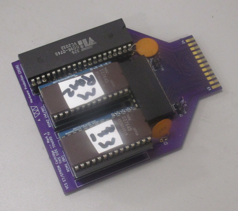
I wanted to run a modern "demake" of Myst for the Atari 2600/VCS on actual vintage 1980s cartridge hardware. The target was the M-Networks "E7" chip that allowed 16k of ROM and 2k of RAM, but it turns out possibly no one had ever used all 2k of RAM before. In theory it should have been as easy as getting a Burgertime cartridge, swapping out the ROMs with my code, and upgrading the SRAM chip from 1k to 2k. This turned into a multi-year ordeal but in the end (spoiler) I did get it working.Background on the Myst demakes
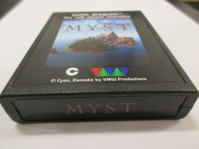
As a fun followup to my Apple II Myst demake I thought I would see how much of the game I could fit on the much more hardware constrained Atari 2600/VCS. As a reminder, the original MYST was one of the first CD-ROM games with hundreds of megabytes of pre-rendered graphics, and generally Atari 2600 cartridges maxed out at 4k, maybe 32k if you did complex bank-switching.The Atari VCS version ended up being a limited subset of the original game (although the full speedrun route is possible). This version ended up unexpectedly popular and got a lot of press coverage.

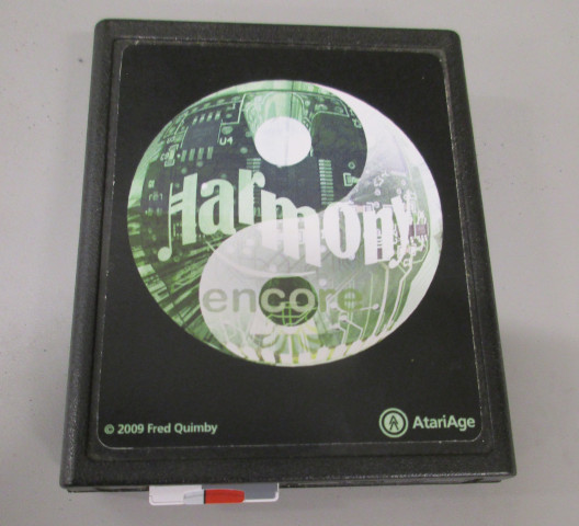
Running on a Harmony Cartridge
The demake was developed on Linux and tested via the Stella emulator. It does run on real hardware. You can test it with the Harmony Cartridge, with is an emulated cartridge that can run ROM files off of an SD card. I also had a custom cartridge made, but this one too is emulated with a Melody board which is similar to the Harmony cartridge, just running the ROM off of flash.These cartridges have 70MHz 32-bit ARM microcontrollers on them handling the bank-switching and other signaling needed to emulate high-end cartridge mappers. This is great for development, but not something that would have been available back in 1977 when the console debuted. In fact the ARM chip inside of it would have had workstation to supercomputing amounts of power back then.
I began wondering, could I get Atari 2600 Myst running using 1980s vintage technology without any ARM micro-controllers?
Fitting Myst into a 16k Cartridge
The Atari VCS lasted a long time, and toward the end of their run companies started using advanced bank-switching to fit more ROM onto a cartridge than the natural 4k limit. The Atari VCS/2600 has the 6507 processor in it, which is a 6502 chip but in a pin-reduced smaller package to save money. It only has enough address lines to access 8k of memory, but the A12 line is used to select between internal addresses and the cartridge which limits programs to 4k. Most early games were 2k or 4k ROMs, but that quickly turned out not to be enough so later various mapper schemes came up to bank-switch larger amounts of storage into the address space..Back in the 1980s you could get cartridges that mapped up to 32k of ROM. Generally chunks of ROM could be bank-switched after accessing special soft-switch memory addresses. Coding for this could get exciting if you were swapping the ROM out in the middle of executing code from it.
The Atari VCS only had 128 bytes of general purpose RAM built in. So just half of the 6502 zero page, and this was also shared with the stack. Some cartridges added extra RAM too, though that was complicated because the cartridge slot did not have the 6502 read/write line available. The way developers got around this was by reserving some address space for reads, some for writes. So you might have a 1k region and so storing to the bottom half would write the value to RAM, whereas if you wanted to read you'd read from the top half, and extra logic involved made sure the read/write pins got set properly for the RAM chip.
To fit as many scenes from Myst as I could I needed to use compression, but due to the race-the-beam nature of the graphics it would be much easier if I could decompress the graphics to a staging area bigger than 128 bytes. When you enter a new level the compressed graphics data is copied to the 256-byte RAM window. Then the ROM is swapped out and the 1k RAM range is banked in, and the 256-byte RAM is decompressed to the 1k range.
The E7 M-Network "Big Game" Mapper
For Atari VCS MYST I picked the E7 "Big Game" mapper from M-Networks (Mattel). Released in 1983, this chip could not only handle 16k of ROM, but also it (in theory) supports up to 2k of RAM. Your primary ROM was 1.5k at the top of the address space that is always mapped in. By hitting a set of soft-switches near the end of memory you could map in 7 different 2k chunks of ROM at the bottom of the address space. You can also swap in 256 bytes of RAM in the remaining 512 byte space (the bottom half for writes, top for reads). Finally, instead of ROM, you can bank-switch in an additional 1k of RAM to the bottom address space.This mapper seemed like a good fit for the Myst demake. The question was where I could get such a chip?
In the table below you can see that only a few games were released using the chip before M-Networks was shut down. Of these, Burgertime is the only one of these that used the RAM functionality, so it seemed like a good source to get a chip.
| Game Name | Commercial Release | Ram on Board | 256 byte bank usage | 1k bank usage |
|---|---|---|---|---|
| Bump 'N' Jump | Yes | None | N/A | N/A |
| Masters of the Universe | Yes | None | N/A | N/A |
| Burgertime | Yes | 1k | 1 bank used | no |
| AD&D Tower of Mystery | No | 2k | many banks used | no |
| In Search of the Golden Skull | No | 2k(?) | ? | ? |
| Locomotion | No | 1k(?) | ? | ? |
| Game Name | Commercial Release | Ram on Board | 256 byte bank usage | 1k bank usage |
|---|---|---|---|---|
| Myst | No | 2k | 1 bank used | YES |
| Elite | No | 2k | ? | YES |
Obtaining Many Burgertime Cartridges
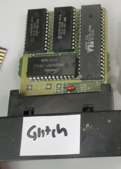
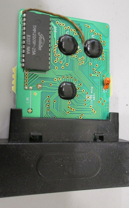
Just to be safe I acquired a bunch of Burgertime cartridges. There are two variants: one with through hole chips (Made in USA) and one with epoxy blobs for the E7 and ROM chips (Made in Singapore). I ended up with 6 cartridges (eventually I bought a few more later). Only 3 of them actually ran the game properly, the others glitched or had other issues.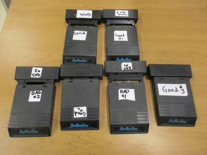
Attempting a Burgertime Cartridge Conversion
In theory converting a Burgertime cartridge to Myst should be as simple as:- Replacing the ROMs with ones with my own code
- Upgrading the RAM from a 1k SRAM to 2k
I tried desoldering the boards with solder wick and a solder pump. That was a mistake. I ended up lifting a lot of pads and losing a bunch of pins. I eventually got a "real" Hakko desoldering gun and it was worth the price.
The ROMs are in the MCM67866 24-pin pinout (same as that for ROMs used in IBM 5150 BIOS and Commodore 64). This pinout *does not* match the standard 28-pin 27C64 8k EPROM format. You can get adapters, and I did some "2364 Adapters" from go4retro but the footprint for the adapters is too big to fit on the existing circuit board.
The RAM is a 1k Toshiba SRAM TMM2009P-25A which is nearly completely undocumented, even by Toshiba back in the day. It was used a few other retro systems and it can be seen that the pinout is essentially the same as that of the more common 6116 2k SRAM so the hope was one of those could be dropped in place. (Note from later: no, no it couldn't).
To try to test things out I made the below monstrosity out of the
harvested poorly desoldered chips. Some of the chips lost their pins
in the process so were soldered into sockets so they'd still work.
The E7 chip was left on the board, and a ribbon cable was made to
grab the signals from the ROM socket and take them to the breadboard.
A testing clip was used to get a few additional signals.
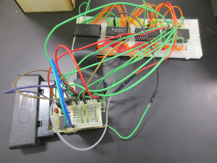
If this had worked with the existing Burgertime chips then in theory it would have been straightforward to swap out the RAM/ROM in order to play Myst!
As you can guess, it didn't work. Though someone on atariage later theorized that if I had thrown enough decoupling capacitors on there it maybe could have worked.
Delaying Two Years
Life got busy and that's where this project stood for 2 years.But then I picked it up again Summer of 2026.
Custom PCB
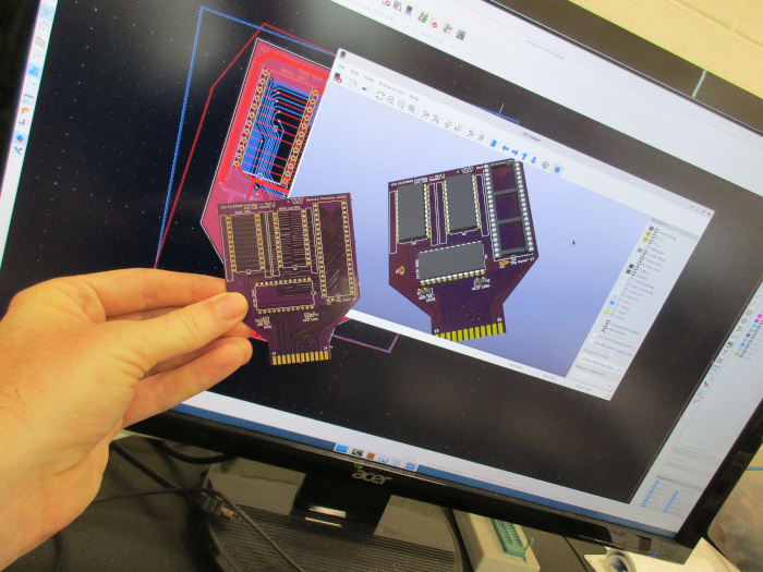
After the long hiatus I finally had some time to restart this project.Since trying to use the existing cartridge was a dead-end I decided it was time to make a custom printed circuit board. I fired up KiCAD and made a replica E7 cartridge, but with extra spacing to allow the ROM adapters to fit and also brought out some extra pins for debugging.
This was my first major project with KiCAD. I previously had used gEDA for things like this, and it took a bit of getting used to. I mostly missed autorouting. I never auto-routed entire projects, but it could be nice sometimes to use it on troublesome signals to get some hints on what might be workable paths.
I got something reasonable put together, then it was time to send it off and wait a few weeks for the finished project to arrive.
Populating/Testing the PCB
Time to see if my board worked.Step 1: Populate board with chips from known-good Burgertime Cartridge
It works!
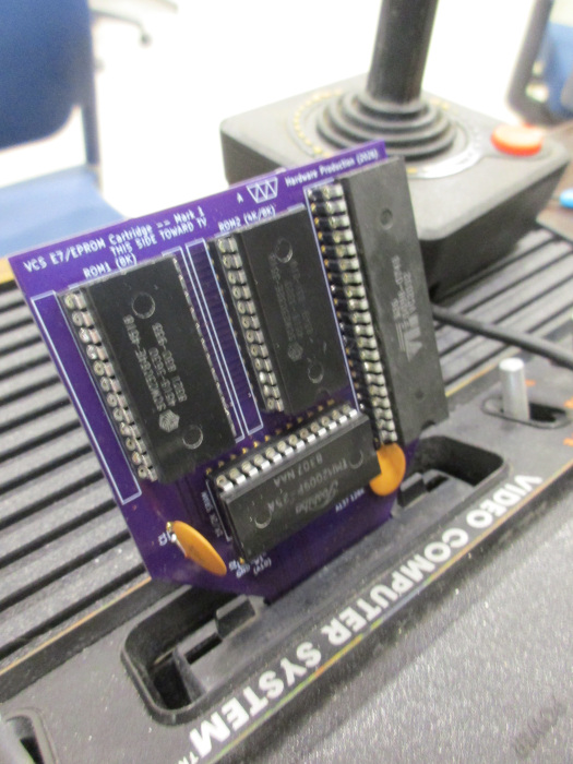
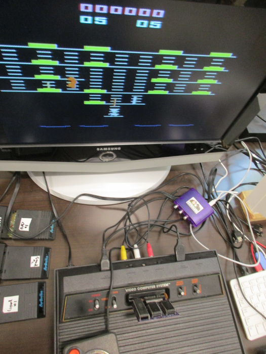
Step 2: Try using burnt EPROM copies of the game using the adapters
Burning a 27C64 8K EPROM in my minipro burner using Linux.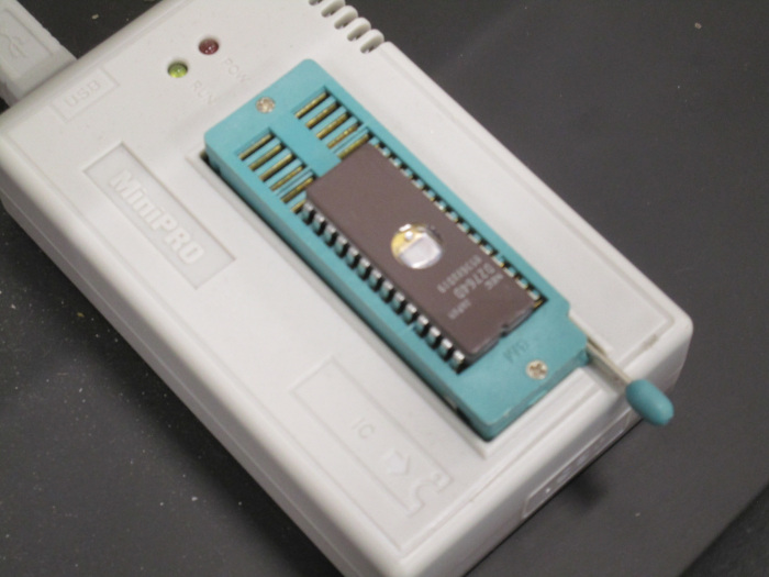
One of the EPROM to ROM adapters I'll be using. Notice it is a lot
wider than a 24-pin DIP socket which is why I had to make the custom
PCB.
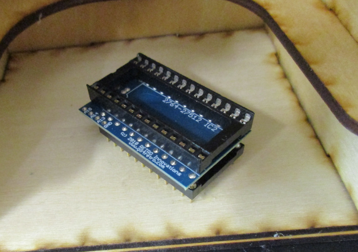
Here's the board populated with the EPROMs. You can also see I only
had large 0.1uF capacitors and yes they were continually getting
in the way.
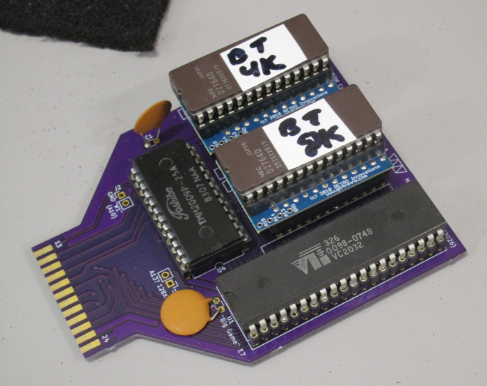
Firing it up, and it works!
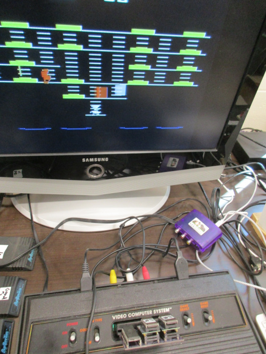
Step 3: Try updating the TMM2009 1k SRAM to 6116 2k SRAM
It didn't work. Oh no.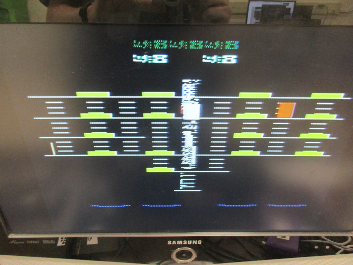
Tried running a burnt copy of the MYST ROMs, just in case it might work.
The title screen worked but whenever it tried to hit the RAM
it would glitch out.
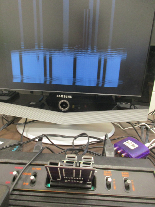
So things aren't working, time to debug.
Writing the first E7 Tester ROM
To figure out what's going on needed to isolate exactly what was breaking when using the 6116 RAM chips.So I wrote a tester in 6502 assembly that would do some reads/writes when you press the joystick buttons. That sounds like a relatively simple thing to write, but on the Atari 2600 nothing is easy. I'll spare you the rundown on things, but it only has 128 bytes of RAM, the closest analogue to a framebuffer is 20 bits (that's bits, not bytes) and you have to draw each 60Hz frame by racing the beam. So just doing the equivalent of a printf() of a memory address involves careful cycle-counting and byte-rationing.
Also on the E7 cart the always-mapped in area is only 1.5kB of code, and
fitting things in that size is also a challenge. It doesn't help that
I wasted a fairly large chunk of it for this really cool title screen:
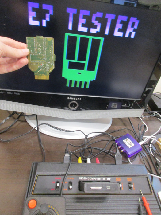
With the original 1k SRAM installed, the test worked fine on all four 256-byte chunks. Accessing the 1k chunk didn't, but that was expected as it didn't exist.
Alarmingly it would reset a lot when the 6116 2k SRAM was installed, almost like it was fighting the bus.
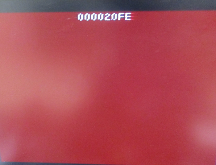
The testing code would try to write values to all of the RAM areas, then read
them back, then have the screen go red with an address if unexpected
values were read back.
Most of the tests failed with the 6116
RAM installed, so it looked like I'd have to write a better test.
Checking on Atariage Forums
I gave regular updates on this project on the atariage forums. I even got responses from kevtris (who is the one who originally described the E7 mapper behavior in his well-known mappers document). I also got feedback from some developers who have also written E7 games.It turns out most of the E7 reverse engineering work happened 25+ years ago and so details were fuzzy and it was suggested I break out a logic analyzer.
Time for a Logic Analyzer
I know it sounds unlikely but I didn't have a logic analyzer in my lab. I had an ancient bus pirate but that was never the best, so I ordered one of the cheap sparkfun usb logic analyzers. While I was at it I also ordered some 28C64 EEPROMs (electrically-erasable, rather than UV erasable 27C64) mostly because I don't have a UV-eraser and I was blowing through my stock of blank 27C64s pretty quickly.Back to the waiting game for packages to arrive.
Revisiting the RAM situation with the TMM2116 2k SRAM
While waiting I looked into the RAM situation again.Toshiba actually sold a lot of models of 2k SRAMs, it seemed plausible that something made by them might be a better match to their 1k RAM than the 6116 by a different manufacturer.
I picked the Toshiba TMM2116 as one to try. Data sheets for this chip do exist, and looking at them it turns out that its signalling is different enough from a 6116 it plausibly could be causing the issues we were seeing.
So I ordered some TMM2116 chips, from two sources on e-bay. Tracking through the USPS can be frustrating, one chip was coming from nearby, one from California. They managed to pass in the system and the one from CA got to the local distribution hub a day after the other but still arrived a day earlier somehow.
Testing the TMM2116 2k SRAM
Sadly it didn't work, though it works better than the 6116 RAM did.Burgertime now works, and all four 256-byte RAM banks access fine.
Enabling the 1k RAM window though makes all RAM (including the 256-byte window) not work. Myst gets much further, but the actual gameplay glitches.
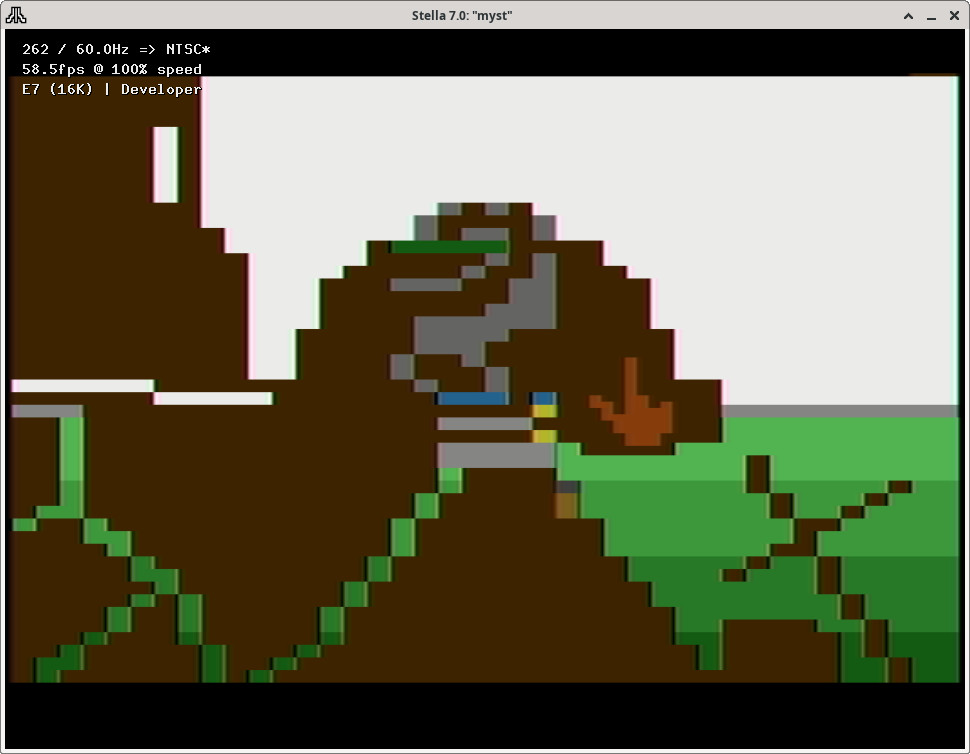
Proper myst level in stella emulator:
What is looks like with TMM2116 chip in:
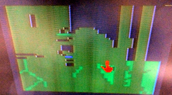
Here's a bit of info on what is going on in the Myst game.
- The title screen / intro loads fine as it only uses ROM BANK5/6
- The linking book at the start runs fine as it only uses some of the 256-byte RAM window for animation. It decompresses data from ROM BANK6 to RAM 256-bank0
- The actual gameplay is more complicated:
- First it copies 256 bytes of compressed data from ROM to 256-byte RAM (it can't decompress directly from ROM to 1k-RAM as the extra ROM pages and the 1k RAM window can't be mapped at the same time)
- It then enables the 1k-RAM window
- Next it decompresses the 256 bytes of data from the 256B RAM window to the 1k RAM window. The decompressed data describes how to draw the screen and is roughly 512 bytes of playfield graphics, colors, sprite overlay, and missile overlay.
- Finally it copies the first 16 bytes of the decompressed data to the zero page (this holds the level config info)
Writing a new E7 Test ROM
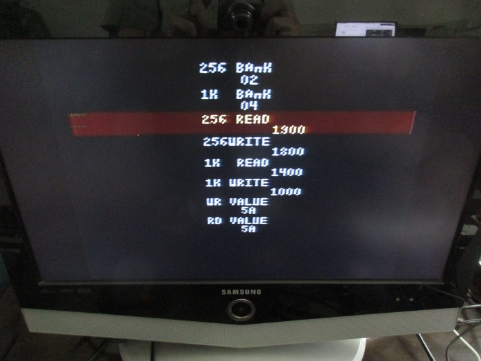
To do some better testing I needed to write a better test ROM. Sadly I had to get rid of the fancy title screen to make room. This new one lets you pick the various bank-switches, as well as picking the addresses to read and write and you can adjust the addresses by hitting left/right on the joystick, and can trigger reads and writes by firing the joystick.
Here's the new interface:
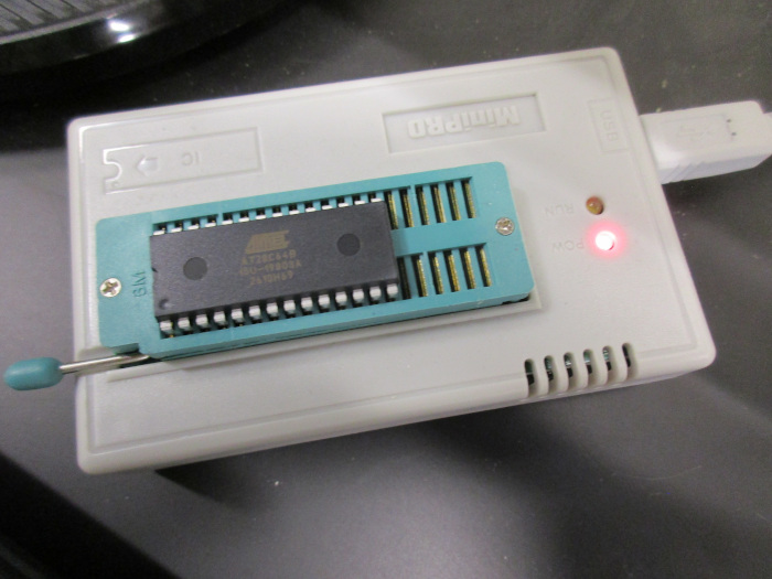
And here I am burning it to one of the new 28C64 EEPROMs:
Finally Using Logic Analyzer
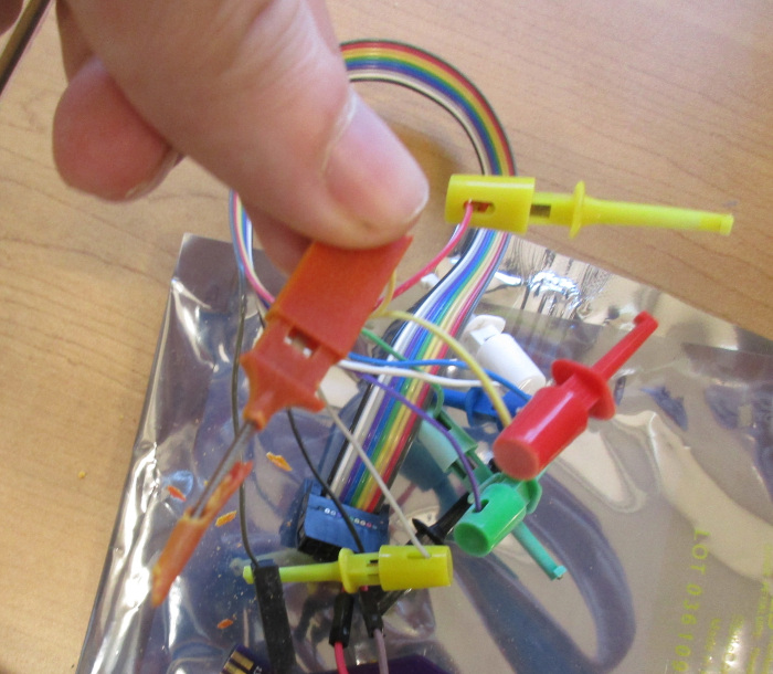
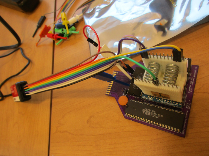
As I mentioned I got one of the cheap Sparkfun USB logic analyzers. It doesn't really come with test probes as much as just some female-female jumper wires. Luckily I did have an old 24-pin DIP test clip that a retiring colleague had left me, which helped.I also needed some individual test probes. I tried using my old bus-pirate test clips but they had been sitting in sun 10 years and the plastic disintegrated.
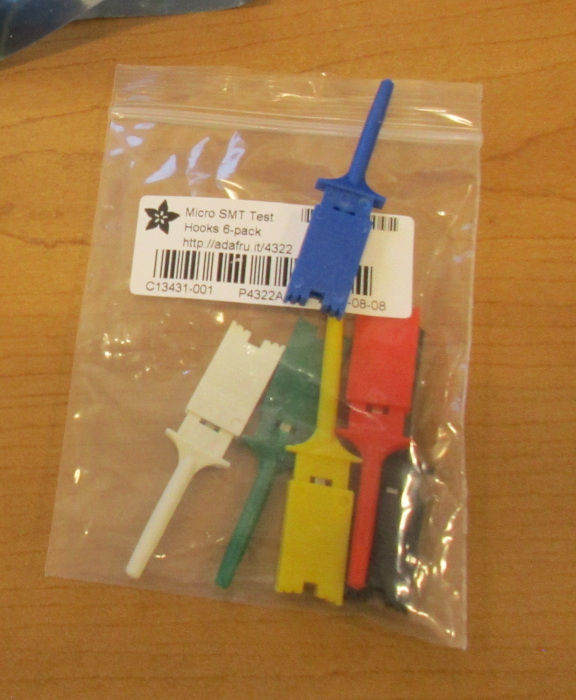
Luckily I raided my pile of neglected adafruit purchases and found some clips still in bag that I soldered onto and could use.
Disintegrated test clip:
Lucky stash of new-old stock test clips:
Here's what the test rig looked like for the initial tests,
though possibly I had it wired
up wrong for this picture but eventually remembered where pin1 was.
Initial Logic Analyzer Results
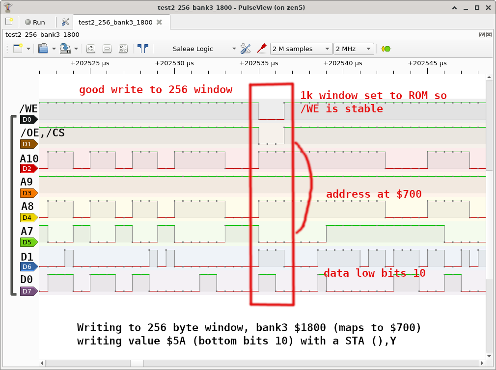
With only 8 pins to work with for these first measurements I tried to pick a subset that could tell me what was going on.
Here are the results with ROM banked in and a write to the 256-byte window
showing a working write to the SRAM. All of the various signals
seem reasonable:
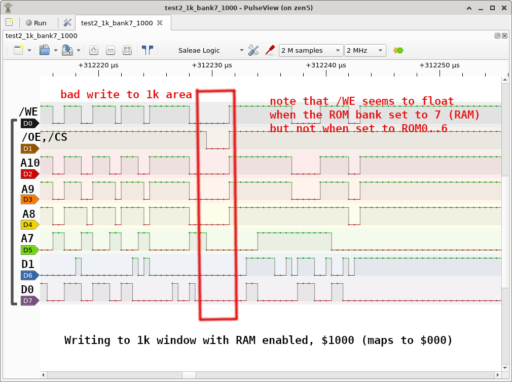
Here is a write when the 1k-RAM bank is enabled, which doesn't work.
In this case the /WE (write enable, active low) signal seems to either
be floating or otherwise going low a lot of times that it doesn't
during the good writes. We'll come back to this later.
More SRAM doubts
About this time is when I discovered there were unreleased games that had used the E7 mapper (see the table at the beginning of this document). There were pictures of some of these, and they actually had 2k of RAM installed.The best documented one is AD&D Tower of Mystery where you can clearly see it is using Toshiba TC5116 2k SRAM.
There is a data sheet available for this, and it turns out it does have slightly different behavior on chip selects than the TMM2116 we were using.
Since in theory this was a real working prototype for an actual working game, maybe this is the secret to getting things working?
So I ordered some in hopes I could drop it in and solve my problems. (I ordered on e-bay. I tried to order from American supplier for a quicker response and to maybe avoid counterfeit parts from overseas, but it took long enough that I am pretty sure the vendor was just drop shipping from China and it took forever to arrive. So I ordered more chips from another vendor and of course they all more or less arrived the same day). As an aside, if you're upset about current DDR5 prices, just know I paid $5million/gigabyte for this RAM.
I dropped in the new RAM... and it failed the same way the 2116 did. Urgh.
It would have been nice to have better pictures of the unreleased prototype games, epsecially of the traces on the back. The AD&D prototype board not only has 2k of SRAM but it has a different layout from Burgertime and is using 28-pin EPROMs as well. From the picture online it also appears that the /OE and A10 lines are connected, which is an odd thing to do and would only work if only the 256-byte ranges were used.
I later investigated the source code for that game and sure enough it only uses the 256-byte ranges, it never uses the 1k range. So my hopes for proof that someone else has used the full memory range of the E7 were squashed.
TODO: maybe show the different decoder layout diagrams for the three memory chips.
E-mailing people who were there
While looking at the prototypes I raelized that one of the authors of the "AD&D Tower of Mystery" prototype was still around and on the internet. So I e-mailed them and asked if all 2k of RAM ever worked on the E7 board.They actually replied, but said it had been so long they can't remember much about the E7 chip. Though they did say that when coding they'd max out whatever resources were available... which could in theory imply it didn't work or else they would have.
Back to the Logic Analyzer
I decided it was finally time to try to get more complete coverage of read/write operations using the logic analyzer.I was triggering on the RAM /OE line as that's the easiest way to find SRAM accesses in the huge pile of signals.
The logic analyzer can only probe 8 signals at once, which is limiting as ideally we'd track most of the 40 pins on the E7 chip.
I did things in four batches. This allowed measuring all but two of the pins (I was too lazy to do a fifth batch for just those two pins). I only had a 24-pin test clip so I had to move that halfway through the testing.
I set the analyzer to read 20 million samples at 4MHz. (The 6507 in the Atari VCS runs at 1.19MHz so not a nice even multiple. I also wasn't sure how fast to sample as I am sure there are some sub-cycle timings going on that might be relevant).
I won't show all the results, but some interesting highlights for the curious:
- The 128k pin does seem (as theorized) to be the OR of the ROM0 chip select and the ROM1 chip select (for use if you want to use one 128kbit [16kB] EPROM instead of two 8kB ones)
- The NC pin is possibly the A13 pin if you want to use 16kB EPROMs but I didn't test enough addresses to verify
- The ROM0/ROM1 chip selects are never active when the RAM one is, which negates the theory maybe somehow the problem is that they are left active when RAM is going
- The address lines for the SRAM always seem to give the proper expected values for accessing the various memory regions
- I verified the weird issue that with the 1k RAM enabled the /WE line seems to almost be masked with the RAM-A8 signal rather than holding high when RAM /OE is high.
- When reading the data bus it was clear that when the 1k RAM area is active, the value the CPU tries to write to memory is somehow disappearing and never makes it to the data bus. Odd.
- The A12 (cartridge select signal) does not match what I expect, with it low when I'd expect high. I might be misunderstanding what's going on though because otherwise nothing should work if somehow that is broken.
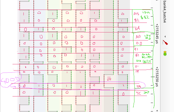
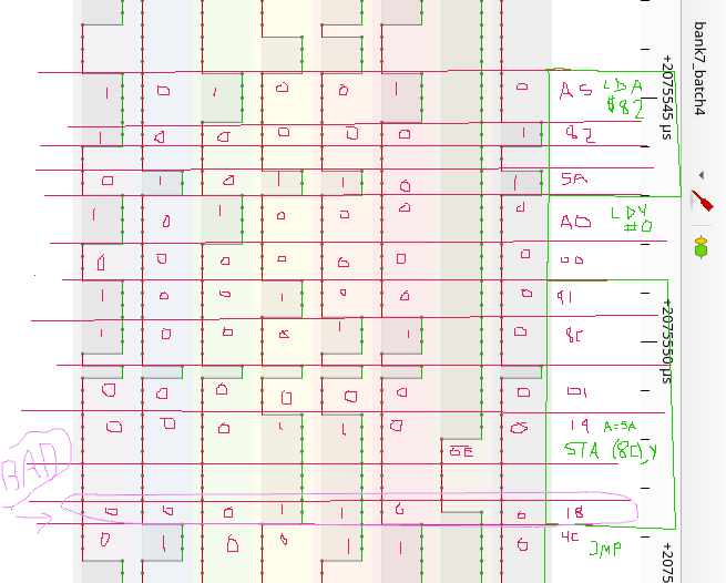
I had to refresh my 6502 knowledge to know what to expect on the data bus. For the write I was doing essentially a STA ($82),Y indexed write. This takes 5 cycles. This should look like:
- $91 - the opcode for the STA instruction being read from the PC
- $82 - the address from the zero page we are loading the address from
- $01 - the low byte of the address
- $18 - the high byte of the adress
- $5A - the value we are writing out to SRAM (from the accumulator register)
Here is an annotated trace showing a working 256-byte load, plus some of the preceding instructions showing the setup. Sorry for the hand annotations, I was using the GIMP and for some reason the font/text tool is really a pain to use with current versions. Note: I have the address as $1901 instead of $1801 for the write, that's a typo it should be $1801.
And here is a not-working write transaction showing the missing $5A value from
the CPU.
Instead what gets written is the unchanged $18 from the previous cycle,
maybe implying the bus was left floating with the previous value?
I went back and looked at the signals, and yes the /WE issue is
still present:
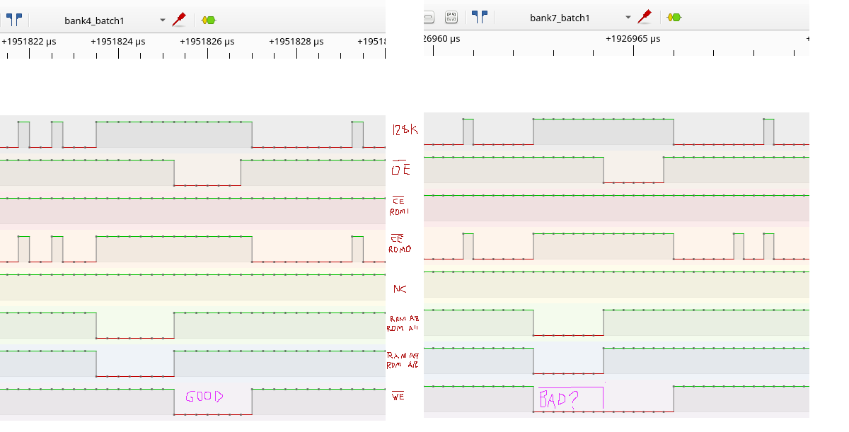
In case it was somehow the chip leaving /WE floating I did try hooking a weak pullup (10k to 5V) to the /WE pin, but that didn't change anything so it looks like the E7 is actively driving the weird signal on /WE we are seeing.
I double checked the TC5116 datasheet, and the /WE signal being low before /CS,/OE going low should just tri-state the data output lines so I would think that /WE being low earlier like shown shouldn't affect things, but it does seem to be the only obvious difference between the working and not-working test cases.
Trying an OR gate
Since a pullup didn't help, one thing that might work would be replacing the /WE line going to the RAM chip with a logical OR of the /WE and /OE lines. That would at least make that signal match more closely what the "working" trace looks like.
I guess I should check my stash of ICs from my childhood
(yes I did electronics as a kid, mostly based on Forrest Mims books from
Radio shack). They've been sitting there in my
"IBM PC Network Baseband Extender" box in anti-static
foam being lonely the past 30 years. It's mostly 7400 and 4000 series
logic, 7-segment LED displays, 555 timers, 3909 LED blinkers, and 741 op-amps.
Mostly sourced from Radio Shack, JDR micro-devices, and
some rescued chips scavenged from Apple II machines my high school was
getting rid of.
If you look closely mixed in are the parts for the sadly never-realized
plan to build a custom z80 computer based on some TAB book acquired at a
local library booksale.
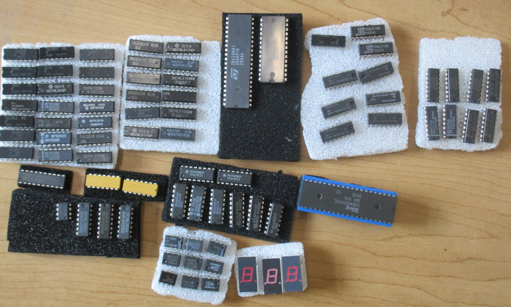
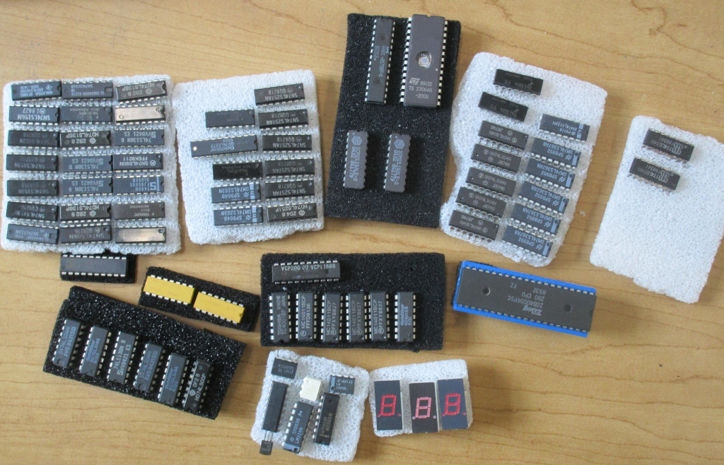
I apparently had foresight and the 74LS chips were ordered by part number.
After more trouble than it should have been I found a 5V supply and
verified the chip was still OR-ing after all these years:
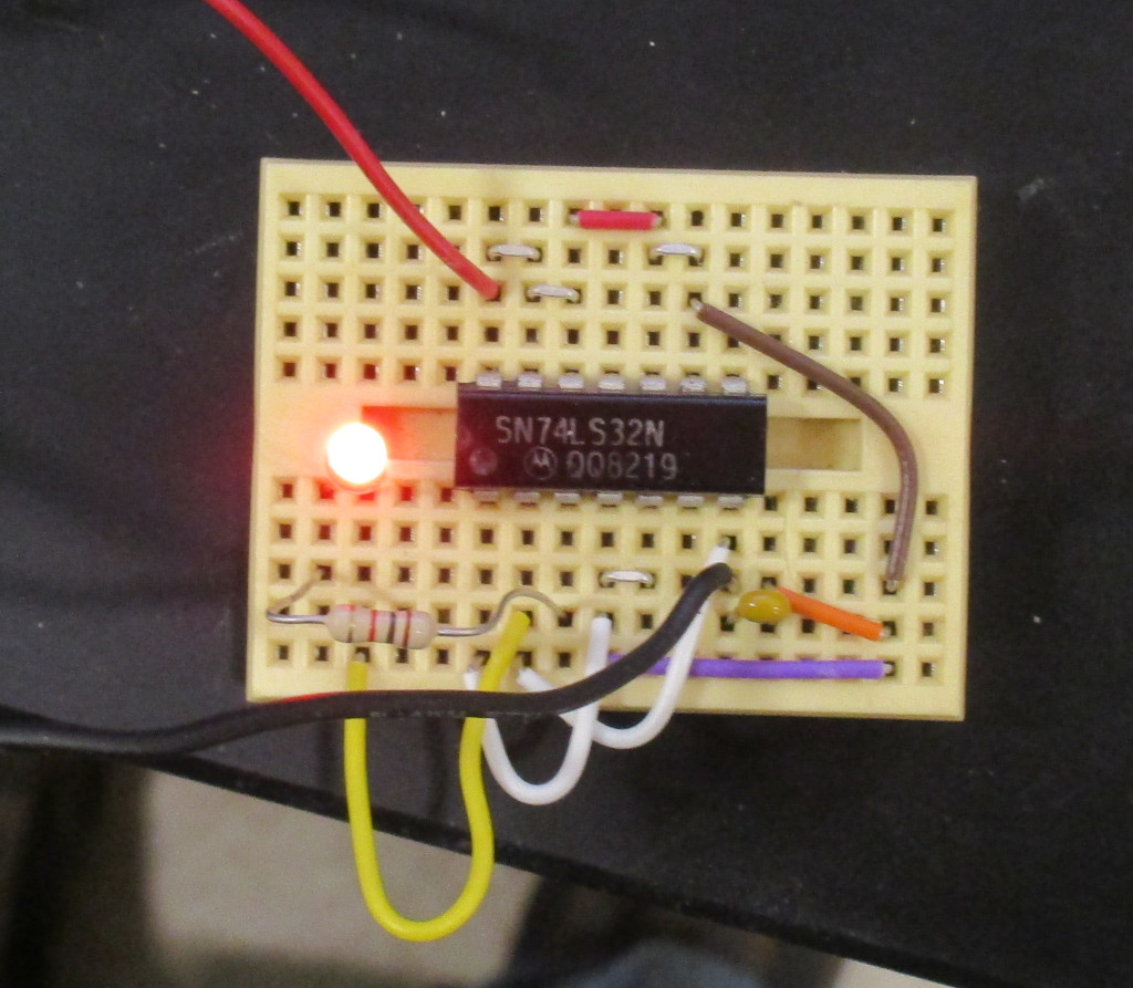
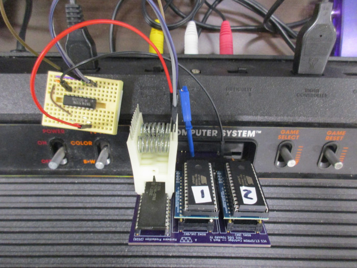
So I lifted the /WE pin on the RAM and then hooked up the OR-gate.
Sadly, things still didn't work.
One Last Attempt with the Logic Analyzer
I ran the logic analyzer with the OR gate attached. The /WE signal now looked the same in the RAM and no-RAM case. Still not working.I then *completely removed* the RAM chip and tried looking at traces. When doing a write the data bus is definitely not getting the $5A data to write. So it's not the RAM chip messing with the bus, it's something else.
Quite possibly it's the E7 chip itself (it's a mystery why it even has the data lines going into it because they shouldn't be necessary). It's weird though as the data lines come right from the 6507 on the Atari, the E7 chip isn't able to tri-state or intercept them. (though it could be accidentally or on purpose driving values onto the data bus when it shouldn't be).
One Last Longshot
I've run out of summer so won't have much time to work on this more.I had been thinking, if it's the D7..D0 data bus being driven with the wrong values, and those seemingly are being messed up by the E7 chip itself, why not just leave them unconnected?
So I used some pin headers to extend the socket for all pins except the
data bus:
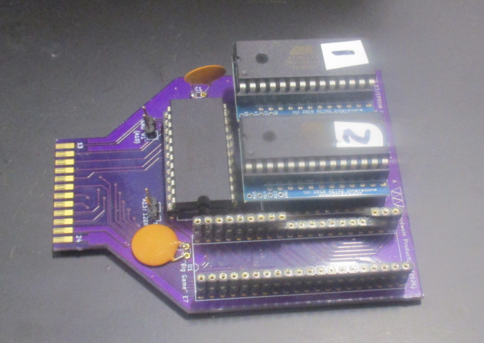
It's hard to tell but those 8 pins aren't touching.
Tempted to make a "floating bus" joke here. Really, they probably
should be pulled to ground or something.
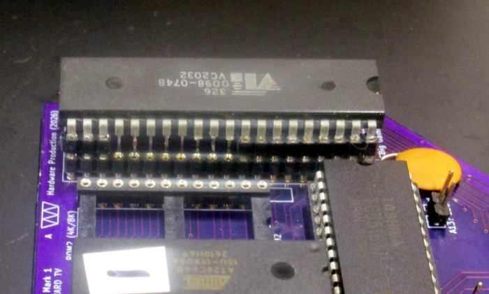
And now to fire it up....
Success!!!!!
With the data bus disconnected, the E7-test program let me read/write RAM properly even with BANK7 in!!!Next step was to put the Myst EPROMs in. Which I managed to do upside-down (ugh). But I fixed that... and it worked! Finally!
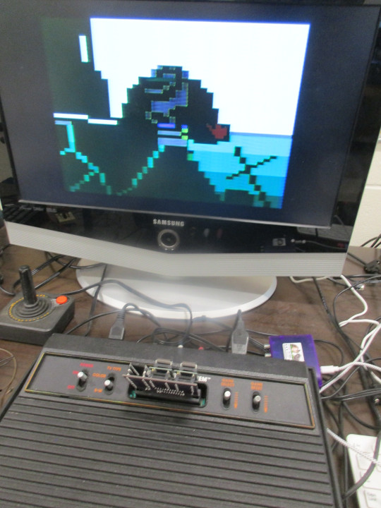
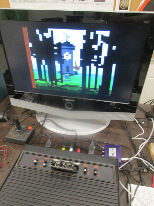
Weird that I might be the first person to ever successfully run an E7 mapper using all 2k of the SRAM. And if I'm not, I'm probably the first person to do it in the last 40 years.
As a summary, what it took to get this working:
- The E7 chip from a burgertime board, with the D7..D0 pins not connected
- SRAM upgraded to a 2k Toshiba TC5116 (note: a TMM2116 might also work but haven't tested yet)
- ROM adapters to convert the pinout from the 24-pin mask roms to 28-pin 27C64 EPROM
Increasingly Desperate Things I was Considering
I never give up easy on these projects so I had been considering a few extra steps if it hadn't ended up working:- Try to track down someone who worked at M-Networks who remembers useful details about the E7 chip
- Obtain one of the other E7 carts (Masters of the Universe?) and see what kind of E7 chip is in them. This is not optimal, just opening the cartridges non-destructively is nearly impossible. I had actually given in and currently there are Bump 'n' Jump and Masters of the Universe carts slowly making their way here. However I am 99% sure that since they were made in Singapore they'll be the COB/epoxy-blob variants.
- Take an epoxy-blob E7 chip, saw it up, and wire up the pins to a 40-pin socket to see if it's a newer version that would work
- Find someone to de-cap the various versions of the chip (epoxy or otherwise) to see if any of them might be newer revisions
- Maybe give up and assume the E7 mapper was just broken with the 1k RAM range enabled, but since no games used it, it didn't matter if they shipped the broken chips. Maybe it was fixed in a later revision but who knows.
So Why Did You Do This? And What Now?
Part of it was just curiosity.Another part was things like the demoscene. Some competitions prefer if the code you write actually runs on real retro hardware rather than some sort of fantasy console. Until I proved the E7 actually worked with 2k, using all 2k in a demo could vaguely be deemed an unproven fantasy setup.
Possible future work:
- Work on another game / demoscene demo
- Design a new circuitboard that has the disconnected data lines and also has the proper pinout for the EPROMs so I don't have to use the current bulky hacked-up board.
- Could also see if I can get 16k EPROM support working (rather than having two 8k ones)
Resources
You can get the source code for the tests, as well as the KiCad files from the boards inside of my Atari VCS git repository under the testing/e7* and hardware/e7_cart directories respectively.Back to the Atari 2600 Myst page
Back to my Apple II / Atari 2600 Demakes page
Back to my homepage